

Embedded ADAS Algorithm Optimization with High-Performance DSP IP and CV Software Library
It is a challenging task for algorithm developers to be able to map a state-of-the-art vision algorithm derived from theoretical research to performance-optimized software that is running in real time on an embedded platform. In this paper, we take the implementation of the ADAS lane-detection algorithm as an example to present the embedded CV software-development flow and the challenges facing CV algorithm developers to achieve high-performance under constrained system resource. We further showcase how a feature-rich, performance-optimized CV library can be used to reduce the software-development cycle to only a few weeks from having generic functional C code to DSP-optimized code that supports high-performance vectorized computing in real time. Finally, we demonstrate how to optimize CV software using advanced features offered by high-performance embedded vision DSPs, represented by Cadence’s Tensilica Vision DSP family of products.
Introduction to Embedded CV Software Development Flow
Recently computer vision (CV) technology has seen a rapidly increasing rate of adoption in the application of autonomous driving. CV algorithms are very compute intensive. Deployment of the algorithms often requires specialized high-performance DSPs or GPUs to achieve real-time performance while maintaining flexibility. It is a challenging task for algorithm developers to be able to map a state-of-the-art vision algorithm derived from theoretical research to performance-optimized software that is running in real time on an embedded platform.
CV application development for embedded systems is often severely constrained by the computation and hardware resources of the corresponding systems, as well as the real-time operating conditions under which the systems are utilized. Embedded developers must be able to optimize the performance of their applications within the constraints imposed to the systems. Performance metrics in terms of data processing throughput and accuracy have to be balanced with other optimization objectives, such as code/data size, memory footprint, latency, and power consumption.
The process of embedded vision application development typically consists of five steps, shown in Figure 1.

In this white paper, we briefly touch on the characteristics and challenges of lane-detection algorithms. Then we turn our focus to the implementation and optimization of the algorithm in steps 3 and 4, using the Tensilica Vision DSP and the corresponding DSP-optimized CV library, XI library.
Implementing a Robust ADAS Lane-Detection Algorithm
The lane-departure warning system (LDWS) has been an essential function to the realization of an ADAS system for autonomous driving. Almost every LDWS starts with a lane-mark-detection phase that can be generalized and simplified with the following key steps:
- Road feature extraction
- Post-processing for outlier removal
- Tracking filtering and data fusion
The accuracy and reliability of LDWS depends on the accuracy and robustness of the lane-detection algorithm, which must take into consideration the shapes of the lane marks, non-uniform texture on the road surface, lighting conditions, shadows and obstructions, etc., while computing in real time following the high-speed movement of the vehicle. In this paper, we present a robust lane-mark-detection algorithm that deploys multiple CV processing steps to enhance the robustness of the detection.
As shown in Figure 2 and Figure 3, we take a regular video image frame, captured by a camera mounted on the vehicle, to extract an ROI that contains the lane marks. Then an inverse perspective transform is performed based on the camera parameters to bring the lane marks into relatively parallel positions in the image. This is followed by a few image enhancement steps, including filtering, equalization, and thresholding, performed to reduce noise. Next, lane-mark detection and selection steps are performed based on the Hough transform. Finally, the detection is enhanced using inter-frame tracking techniques. The algorithm was prototyped in MathWorks’ MATLAB to confirm the functionality and the performance of robustness.


Algorithm Optimization for Embedded Systems Using High-Performance DSP
While it is relatively straightforward to prototype the algorithm in MATLAB, the effort to port the corresponding algorithmic steps to a real-time embedded system is significantly higher. Due to the complexity of the algorithms, generic C code that processes image pixels sequentially can’t achieve real-time processing speed, unless it is executed on a high-performance compute server that can’t be used as an embedded system with any practical considerations for size and power.
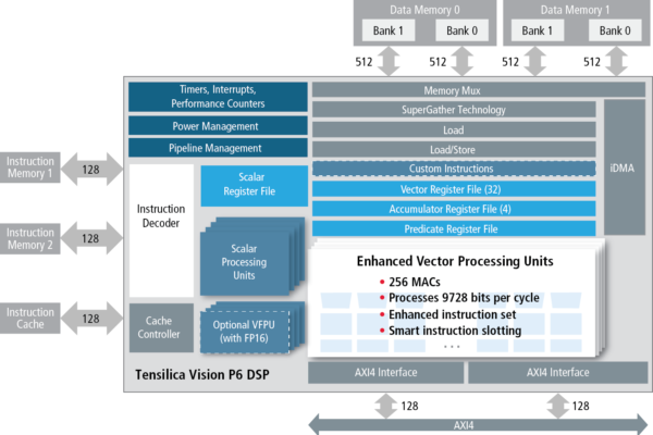
For proof of concept, we have selected the Tensilica Vision DSP IP integrated into a FPGA-based prototyping system. The Tensilica Vision DSP is based on a very high-performance DSP architecture that supports up to 64-way single-instruction, multiple-data (SIMD) vectorized load/store and computation. The architecture encodes and dispatches instruction in the VLIW format. Up to five slots of instructions can be issued and executed in parallel in a single cycle. In addition, a vision-optimized instruction set that focuses on 8-bit or 16-bit parallel pixel processing is deployed to boost the computation performance for vision algorithms. Vision computation is memory bandwidth intensive due to the large sizes of image data.
The Vision DSP integrates a 2D-capable scatter-gather iDMA and two banks of high-speed local RAMs to overcome the memory access bottleneck. This advanced architecture is demonstrated in Figure 4.

(for full resolution click here)
While the architecture of Vision DSP is designed to support high-performance vision computing, the effort to port generic C code to the DSP to utilize the compute capability is not trivial. The Vision DSP is distributed with a high-performance compiler that can infer and extract parallelism from the generic C code. Nonetheless, it is often required to develop the vision-computing kernel functions using hand-optimized C intrinsic code in order to maximize the performance. A rich set of vision-computing kernels have been implemented into a production-quality, OpenCV-like software library called XI to reduce the porting and optimization cycle.
In this study, we leveraged significant number of XI library functions in all the processing steps to perform perspective transform, image filtering, equalization, thresholding, Canny edge detection, and Hough transform, etc., as shown in Figure 5. The utilization of the XI library functions significantly reduces the effort to port and optimize the lane-detection algorithm to the Vision P5/6 Vision DSP. Real-time computing performance can be achieved in the instruction set simulator (ISS) within one to two months.

Throughout the entire flow of the lane detection algorithm, the image data is processed using a technique called tiling with the facilitation of the iDMA. The wide SIMD data processing requires image data to be accessed in tight computation loops from the high-performance wide local RAMs using vectorized load/store instructions. The tiling scheme allows a small portion of the image to be brought into the local RAMs from the much slower system memory, using block data transfer supported by the iDMA.
In order to minimize the impact of the memory access, the implementation also deployed a ping-pong DMA buffering scheme shown in Figure 6. In this scheme, the first iDMA descriptor is programmed to fetch source tile 1 from the DDR Memory to the ping buffer located in the local RAM. After the completion of the DMA transaction, the DSP software starts processing the ping buffer for tile 1. In the meantime, the second iDMA descriptor is programmed to fetch source tile 2 from the DDR Memory to the pong buffer located in the local RAM. Since the iDMA performs the second tile fetch in parallel with the DSP processing, it effectively hides the memory access latency.
The combination of tiling and ping-pong DMA has produced a speed-up factor of 15X to 20X, when the algorithm is executed from the prototyping FPGA hardware target.

Conclusion
In this paper, we take the implementation of the ADAS lane-detection algorithm as an example to present the embedded CV software development flow and the challenges facing CV algorithm developers in real-life applications to select and implement a robust algorithm while achieving real-time performance under constrained system resources. We further demonstrated the superior architecture of the Tensilica Vision DSP IP and how to utilize the high-performance XI software library for rapidly porting and optimizing CV algorithms to embedded hardware targets. The project to develop the ADAS lane-detection algorithm was completed within three months by one software engineer with no prior experience of programming a Tensilica Vision DSP. The tasks included application and algorithm research, algorithm prototyping using MATLAB, developing generic functional C code, optimization to Vision DSP, and demonstration on a FPGA prototyping hardware platform. With built-in support of advanced hardware features like 2D DMA and programming techniques such as tiling and ping-pong buffer management, a highly optimized implementation of the lane-detection algorithm can be demonstrated in real time on a prototyping hardware target with only a fraction of the operating frequency achievable by the Vision DSP in an embedded semiconductor SoC.
About the authors:
Charles Qi is a Senior System Solutions Architect in Cadence’s IP Group, responsible for providing system solutions based on the Cadence Tensilica DSP and Interface IP portfolio.
Han Lin is Computer Vision Application Software Engineer at Cadence.
 If you enjoyed this article, you will like the following ones: don't miss them by subscribing to :

