User interface: A matter of memory
There is a common theme in user-interface design across almost every market sector: the use of advanced 2D and 3D graphics in user interface designs is becoming steadily more prevalent and more sophisticated. This is one-way traffic: once users have gained a taste for digital graphics displays, touchscreen controls and other graphical features, they do not want to go back to an older interface style based on mechanical dials, gauges, buttons and switches.
In general, the more detailed, sharp, attractive and dynamic the graphics, the more users like the interface. This means that microcontroller-based embedded systems of many kinds either are facing now, or are likely to face in the near future, a requirement to deploy a graphics display control platform of some kind. This platform will often need to be scalable to cope with constantly escalating user demand for more, bigger and better graphics and display capabilities.
A crucial element in such a platform is the memory system: the rendering of graphics calls for a large amount of fast memory capacity. Today, this need is typically met by a combination of non-volatile Flash memory for storage of static graphics content, and external DRAM for storage of dynamic content. Internal video RAM (VRAM) inside the microcontroller might in some cases store the most highly dynamic graphics content.
But while such a memory architecture offers proven performance, the need for separate memory interfaces between the DRAM and the MCU, and between the Flash device and the MCU, results in a high pin count, a large board footprint and a complex and expensive PCB. This article shows that the use of a new memory bus technology supporting both Flash and DRAM can address this problem effectively, reducing pin count, board footprint and system cost.
New scope for cost and space savings
The problem with existing memory architectures is best illustrated by reference to an application example: a mid-range instrument cluster in a car’s dashboard.
A hybrid (graphical and mechanical) instrument cluster, featuring graphics rendered on a small LCD screen between conventional mechanical dials and gauges, may be implemented with a memory architecture consisting of a microcontroller-based System-on-Chip (SoC), a Synchronous DRAM (SDRAM) scratchpad memory and a high pin-count NOR Flash memory. The fast NOR Flash memory provides fast boot capability, so that static graphics – such as background wallpaper and speed limit warning signs, may be loaded into the SDRAM and from there rendered by the MCU as soon as the driver presses the Start button or turns the key in the ignition. The SDRAM provides scratchpad storage for slow-changing graphics content with a low refresh rate of around 20Hz, such as the fuel gauge and temperature gauge. Highly dynamic content such as maps and navigation instructions, with a refresh rate of typically 60Hz, will be rendered from internal VRAM.
At one time, this architecture would have made use of a legacy parallel Flash interface such as ADP Page Mode. A 512Mbit-density Flash device in a 64-ball BGA package would typically require a high pin count of around 45 for bus communication, providing data throughput of up to 100MB/s. Pressure to reduce pin count led the industry to adopt a serial NOR Flash interface with a much reduced pin count.
Figure 1 reveals the problem with this memory architecture, however: the external SDRAM and external NOR Flash are connected to the microcontroller via separate buses, and might typically require in total as many as 41 pins at the microcontroller for data transactions. There is a large penalty to pay for this in terms of board footprint, complexity and cost.

with a HyperBus-based architecture (right).
It was to enable a new memory architecture with a massively reduced pin count that the HyperBus™ interface technology was introduced. Benefiting from the development of special protocol and clocking schemes and dedicated techniques for enhancing data integrity, the HyperBus interface is able to offer higher data throughput rates even than legacy, high-pin count parallel Flash interfaces, but to use a low number of pins, as serial Flash interfaces do. What is more, the RAM and Flash memories can both operate on the same bus at high speed, reducing system pin count further.
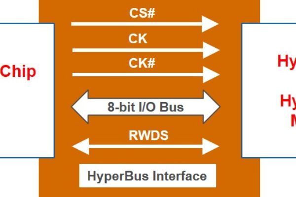
The structure of the HyperBus interface is shown in Figure 2. The bus requires only 12 pins: an 8-bit data bus plus control signals, plus a power input and ground. The devices are selected by a Chip Select (CS) signal. The supply voltage is either 1.8V or 3.0V: this is dependent on the host microcontroller. DDR capability is supported at a reduced speed (100MHz) by either a single-ended clock at 3.0V, or a differential clock at full speed (166MHz) at 1.8V.

a single device (13 if a second device is also on the bus).
The implementation of this HyperBus architecture calls for the use of HyperBus-compatible parts. Discrete HyperRAM™ and HyperFlash™ memory ICs are available from Cypress Semiconductor, each housed in a 6mm x 8mm, 24-ball BGA package. The HyperFlash devices are available in 128Mbit, 256Mbit, 512Mbit and 1Gbit densities, and offer up to 333MB/s read bandwidth in DDR mode. The HyperRAM devices, available in 64Mbit and 128Mbit densities, provide up to 333MB/s read/write bandwidth in DDR mode. The temperature grade is -40°C to 125°C for HyperFlash and -40°C to 105°C for HyperRAM.
Cypress has also introduced the HyperFlash + HyperRAM MCP solution: a system-in-package combining a NOR Flash die and a self-refresh DRAM die in a single 24-ball BGA package. This solution requires 70% fewer pins than the two-chip alternative, reduces board footprint by 77% and offers board design flexibility (see Figure 3).
Cypress also supplies the Amber series of HyperBus-compatible microcontrollers within its Traveo family. Other controllers supporting the HyperBus interface are available from Freescale/NXP, Renesas and Xilinx.
The value of the HyperBus architecture is most clearly expressed by comparisons of data throughput-per-pin. The maximum data throughput from the memory to the MCU via HyperBus is 333MB/s at 1.8V (200MB/s at 3V). The 333MB/s rate is equivalent to 41.6MB/s per pin (333MB/s across eight data pins): a circuit with a similar density but using a Quad SPI Flash interface would offer around half this throughput-per-pin.

and RAM devices by 77% compared to a two-chip solution.
The increased data throughput-per-pin leads directly to a cost saving compared to other high-speed architectures, as it enables the use of an MCU with fewer pins (smaller, therefore cheaper), and a PCB with fewer layers (cheaper to manufacture and assemble). In many cases, users of HyperBus technology will benefit from both this cost saving and enhanced performance when replacing older SDRAM + NOR Flash systems.
The connection between the MCU and HyperFlash and HyperRam in separate packages requires four layers including Vcc and GND (two for the connection). An MCP device, combining the RAM and Flash in a single package, needs one less layer. Interfacing to a Cypress Amber MCU in a Quad Flat Package (QFP), the connections may all be made to pins on one side of the MCU package. When connected to an MCU in a BGA package, more layers would be required (see Figure 4).

on a single or dual layer of a PCB
The cost and space advantages of the HyperBus architecture, then, are clear when replacing an SDRAM + NOR Flash with a HyperBus-compatible HyperRAM + HyperFlash memory solution. This HyperBus solution is ideal for mid-range graphics applications such as the instrument cluster described above.
Table 1 summarises the memory architecture options today for designers of a broad range of graphics display-based user interfaces: from a low-end system based on SDRAM, up to a high-end system using very high-speed DDR2 DRAM. It shows that HyperRAM offers comparable performance to an SDRAM-133 based system, but with a much lower pin count. DDR2 or DDR3 DRAM offers much higher performance than the HyperRAM system, but is also entails a much higher system cost.

HyperRAM solutions in a typical automotive use case.
For full resolution click here
In its HyperBus-compatible product offerings, Cypress has ensured that their BGA package is pin-compatible with all Cypress’s QSPI and dual-QSPI Flash memory devices. For designers wishing to scale up a family of products based on a uniform board layout, therefore, the HyperBus interface offers a simple way to migrate to higher speeds and densities.
And in any circuit, HyperBus technology, and the supporting HyperFlash, HyperRAM and Amber MCU products, offer the best available way to combine high data throughput for advanced graphics rendering with a low pin count and a simple PCB layout which is cheap to produce.
About the author:
Marcel Kuba is Director of Field Applications Engineering, Cypress Semiconductor
Image credits: Cypress Semiconductor
 If you enjoyed this article, you will like the following ones: don't miss them by subscribing to :