ARM offers support for TSMC 7nm manufacturing
The IP set does not include support for extreme ultraviolet (EUV) lithography, which is expected to be deployed later.
“The physical IP platform is available for tape outs in 1H17. We see some engineering samples in 2017,” Ron Moore, vice president of marketing in the physical design group at ARM, told eeNews Europe. However, it is not clear that there is a performance, power or area benefit in selecting the 7FF process over the 10FF process.
The 10FF was a marked scaling over 16FF+ that could produce a 20 percent speed increase at the same power, or more than 40 percent power reduction at the same speed, according to past reports (see TSMC Symposium: 10nm is ready for design starts). But it came at the cost of the increased use of double patterning.
Moore explained: “Basically TSMC has two nodes that are distinctly different 16/14 and 10/7. For TSMC 7nm is the next generation from 10nm. But there are additional challenges such as lay-out rules and the electrical properties of transistors.” You can expand that list to include process variation, routability, analysis for sign-off, timing variation and electromigration. And at 7nm without EUV there will be a requirement for triple patterning.
“We will have to redefine our cells to take account of EUV but 7FF is based on immersion lithography,” said Moore.
Next: Routability
Routability used to be about relieving the congestion of wiring. It still is but at 7nm it has to be done with special attention to voltage drop and electromigration and parasitics have made it difficult to design a power grid. ARM has a developed a power grid architect that includes knowledge of the logic libraries. ARM claims that as a result, a knowledgeable SoC designer can create a power grid that meets their needs within a matter of hours, versus the several days and iterations it may have taken previously.

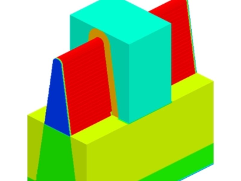
Layout utilization of design before and after using Power Grid Architect (PGA) resulting in 10 percent area reduction and an effective utlization rate improvement of 20 percent. Source: ARM.
However, all of the extra work does mean that an area reduction is not guaranteed.
“The transistors may be smaller, but that does not necessarily mean smaller cells,” said Moore. As has been seen in the past scaling of the front-end-of-line (FEOL) does not produce an area benefit if it is hobbled by an earlier generation of back-end-of-line (BEOL). There are in effect multiple levels of optimisation; transistor, standard cells, IP blocks, cores.
“Area savings can be realized at the core level but it is not a trivial task. It is about optimization for the combination of performance, power consumption and area [PPA].” For example ARM has also had to invent a memory compiler that could utilize a cell-based layout – rather than a more simplistic grid – to minimize variation. Minimizing variation leads to less design margin and better memory PPA.
Moore also accepted that with the move to 7FF comes an increased susceptibility to ubiquitous background radiation and a requirement for additional circuitry. “At 7nm FinFET all memory compilers are ECC and use hardware detect and repair mechanisms. At 16nm it was only for critical or high performance memories with more reliance on software correction.
Next: The big picture
The big picture is that moving from 16nm FinFET to 7nm FinFET you can keep the power budget and improve performance. Similarly, if you move from 16nm to 7nm you can keep a performance level of about 3GHz and drop the power by 20 percent, Moore said.
This power reduction is actually lower than that previously reported for the 10FF process and so detailed comparisons of 10FF versus 7FF are required.
Are there enough benefits at 7nm to make the extra engineering and its impact on yield worthwhile? Xilinx appears to think so and if you want to eventually get on to EUV lithography and you are with TSMC on its roadmap down 5nm and 3nm, perhaps there are.
Related links and articles:
TSMC Symposium: 10nm is ready for design starts
News articles:
Report: TSMC to relabel process as 12nm
Further details of FinFET ReRAM released
Globalfoundries preps 12nm FDSOI process
 If you enjoyed this article, you will like the following ones: don't miss them by subscribing to :