Bond via array technology pushes interconnect boundaries between memory and processor dies to 1,512 pins
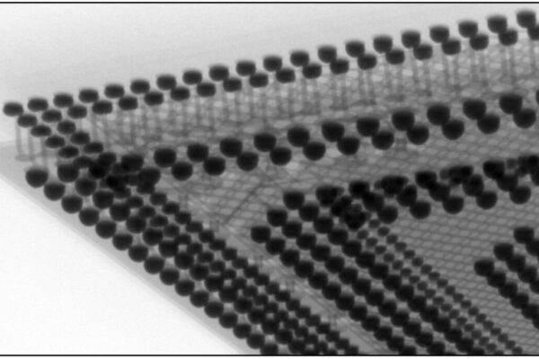
Instead of the traditional solder balls used in solder ball stack PoPs with a pitch limited by the solder balls’ diameter (typically 0.65 to 0.5mm high between PCBs), or even the solder-filled via PoP whereby vias are laser-etched into an over-mould and filled with solder, the bond via array consists in raising 0.5mm high copper wires directly from the metal contacts of the lower PCB, then securing them into an insulation compound that only lets the copper wire extremities stand out about 100mm high for easy reflow soldering. Because the copper wires are so thin, this approach enables a very high I/O density, with a pitch from 0.3 to 0.2mm exceeding what is possible with today’s solder ball stacking and solder filled laser via approaches. By increasing the PoP interconnect bandwidth, BVA technology is positioned as an alternative to Wide-I/O through silicon via (TSV) 3D interconnects, at least a 2.5D solution that is readily available for mobile OEMs while preserving the proven infrastructure and business model of traditional package-on-package (PoP).

Close up of Invensas’ PoP bond via array technology, the copper wires free-standing from the bottom PCB, and their emerging extremities after potting.
According to Simon McElrea, president of Invensas, because it uses common, low cost wire-bond technology, bond via array technology is about half the cost of using TSVs and even cheaper to implement than alternative PoP solutions. But what’s most important is that it does not disrupt the current PoP business model whereby OEMs are free to assemble memories and processors from different vendors. "Wide I/O is a nice theoretical solution to address memory bandwidth and power issues, but the business model does not work yet very well", explained McElrea, "and I don’t think that Wide I/O will be ready by 2013 so what we offer is a bridging technology that OEMs can use now" he added.
Invensas has built and characterized several interconnect solutions respecting the most common PoP perimeter stacking arrangements on 14x14mm packages, demonstrating scalability up to 1512 interconnects with a 0.2mm pitch. BVA PoP is well suited for applications processor plus memory PoP stacks where increasing processor to memory bandwidth will enables higher resolution, faster frame rate video streaming, faster search, higher resolution multi-screen, multi-application operation and a whole new generation of high-resolution 3D applications.
Visit Invensas at www.invensas.com
 If you enjoyed this article, you will like the following ones: don't miss them by subscribing to :