Breakthrough boosts 2D semiconductor photoluminescence
Tungsten diselenide is a single-molecule-thick semiconductor that is part of an emerging class of materials called transition metal dichalcogenides (TMDCs), which have the ability to convert light to electricity and vice versa, making them strong potential candidates for optoelectronic devices such as thin film solar cells, photodetectors flexible logic circuits and sensors. However, its atomically thin structure reduces its absorption and photoluminescence properties, thereby limiting its practical applications.
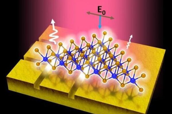
By incorporating monolayers of tungsten diselenide onto gold substrates with nanosized trenches, the research team, led by professor Andrew Wee of the department of physics at the NUS Faculty of Science, successfully enhanced the nanomaterial’s photoluminescence by up to 20,000-fold. This technological breakthrough creates new opportunities of applying tungsten diselenide as a novel semiconductor material for advanced applications.

Wang Zhuo, a PhD candidate from the NUS Graduate School for Integrative Sciences and Engineering (NGS) and first author of the paper, explained, “This is the first work to demonstrate the use of gold plasmonic nanostructures to improve the photoluminescence of tungsten diselenide, and we have managed to achieve an unprecedented enhancement of the light absorption and emission efficiency of this nanomaterial.”
Elaborating on the significance of the novel method, Wee said, “The key to this work is the design of the gold plasmonic nanoarray templates. In our system, the resonances can be tuned to be matched with the pump laser wavelength by varying the pitch of the structures. This is critical for plasmon coupling with light to achieve optimal field confinement.”
The novel research was first published online in the journal Nature Communications on May 6, 2016.
NUS’s press release says that this novel method developed by the NUS team, in collaboration with researchers from the Singapore University of Technology and Design and Imperial College, opens up a new platform for investigating novel electrical and optical properties in the hybrid system of gold with tungsten diselenide. Moving forward, the research team will further investigate the effectiveness of the lateral gold plasmon in enhancing the second harmonic generation and electroluminescence of TMDCs. They will also investigate these effects in other 2D transition metal dichalcogenides with different band gaps, as they are expected to show different interaction mechanisms.
Article originally posted on EE Times Asia. Based on a press release from NSU.
 If you enjoyed this article, you will like the following ones: don't miss them by subscribing to :