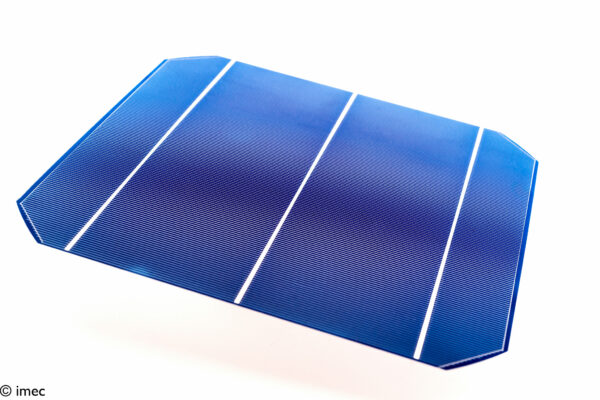
Cheaper solar cells through kerfless wafers
Crystal Solar is a pioneer in direct wafer growing technologies for the next generation of solar photovoltaic products. With nanotechnology body imec, the collaboration has announced that they have achieved a 22.5% cell efficiency (certified by FhG ISE CalLab) with nPERT (n-type passivated emitter, rear totally-diffused) silicon (Si) solar cells manufactured on 6-inch (150 mm) mono-crystalline epitaxially grown kerfless wafers.
[Editor’s note; the term kerf denotes the width of a saw blade or the cut it makes in a workpiece. Conventional manufacture of silicon involves first growing a single-crystal ingot, then sawing it (by steel or diamond-coated wire) into wafers. This is energy-intensive and wasteful of material; even best practice loses nearly half of the grown silicon to the saw cuts. Many efforts have been made, and venture capital invested (and lost) to produce wafers with equivalent quality of monocrystaline lattice structure by some form of alternative process – direct production of the wafer, in effect. Such wafers would avoid the losses to sawing, hence; kerfless.]
Claiming an industry first, imec and Crystal Solar have demonstrated the highest efficiency to-date for homojunction solar cells on epitaxially grown silicon wafers, paving the way toward industrialization of this promising technology.
Crystal Solar’s manufacturing technology called Direct Gas to Wafer enables direct conversion of feedstock gas to mono crystalline silicon wafers by high throughput epitaxial growth. By skipping the polysilicon, ingoting and the wire-sawing steps altogether, this approach not only results in lowest cost/Watt for the wafers but also significantly reduces the capital required to set up a manufacturing plant. Furthermore, this process enables the growth of high quality p-n junctions in-situ which reduces cell making steps while increasing the efficiency.

Imec has adapted its highly efficient nPERT Si solar cell process to align with the properties of Crystal Solar’s kerfless wafers. The 156 x 156 mm cells were fabricated on 160 to 180 µm thick grown n-type wafers with built-in rear p+ emitter. Imec’s n-PERT process included a selective front surface field realized by laser doping, advanced emitter surface passivation by Al2O3 and Ni/Cu plated contacts.
The novel process using all-industrially-available processing steps resulted in record efficiencies for homojunction large area solar cells of 22.5% and a record Voc (open-circuit voltage) of 700mV. This high Voc illustrates the high quality of the wafers and the built-in junction.
Jozef Szlufcik, PV Department Director at imec: “We are extremely happy to have achieved such high conversion efficiencies on nPERT solar cells processed from kerfless wafers using imec’s pre-pilot industrial silicon PV manufacturing line. The combination of our advanced cell process and the innovative wafer manufacturing technique of Crystal Solar, is paving the way for manufacturing of highly efficient solar cells at substantially lower cost and will be disruptive for the complete solar manufacturing value chain.”
“We are pleased to see such a high conversion efficiency on our epitaxially grown n-type wafers with built in boron doped junctions”, said T.S. Ravi, CEO of Crystal Solar. “This approach represents a new paradigm in cell manufacturing with its unique ability to bypass significant steps in both wafer and cell manufacturing thereby dramatically reducing the capex and the overall cost per watt. We expect to achieve >23% efficiencies with imec’s PERT technology in the very near future”, Mr. Ravi concluded.
Imec; www.imec.be
Crystal Solar; www.xtalsolar.com
 If you enjoyed this article, you will like the following ones: don't miss them by subscribing to :