GF debuts 7nm
The process will be in production in late 2018, delivering gate pitches as small as 30nm initially using only today’s optical lithography.
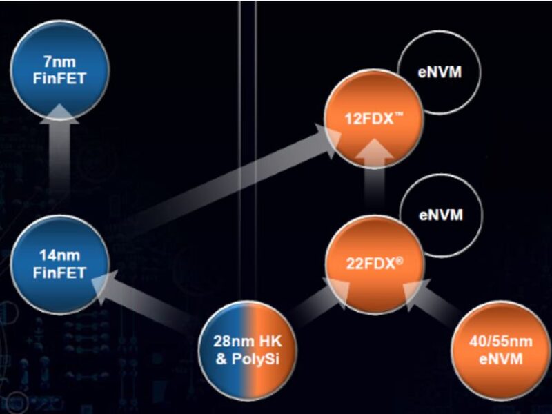
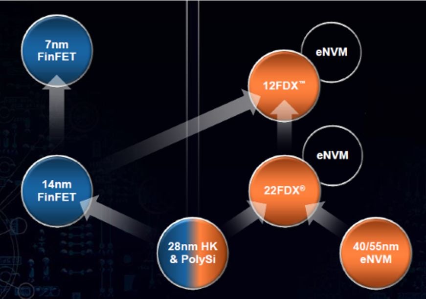
Separately, the company will support a new embedded MRAM in sub-Gbit densities starting in 2018 for chips made in its 22nm fully depleted silicon-on-insulator (FD-SOI) process. The memory technology, licensed from Everspin Technologies, will provide faster write speeds as well as lower power consumption and die size than current variants of embedded flash.
The news boosts the foundry’s competitive position against larger rivals such as TSMC. Both the 7nm and FD-SOI technologies are largely the heritage of IBM’s semiconductor group that officially merged with Globalfoundries in July 2015.
“For the first time we have a differentiated road map…we’re taking an independent view of where the market is going and developing technology for it,” said chief executive Sanjay Jha, a former Qualcomm and Motorola executive who took the reins at the foundry less than three years ago.
“I was TSMC’s biggest customer for a long time, we are not exactly where they are but the progress we have made is remarkable and I think customers are beginning to notice,” Jha said in a meeting Wednesday with press and analyst.
He noted the foundry is still only about half the way to bringing uniformity across its fabs that came from AMD, IBM and Chartered Semiconductor. For example, some things as simple as file-naming conventions still vary among factories.
Among Globalfoundries’ other rivals are much larger companies with leading-edge technology but smaller foundry divisions.
Analysts agree Intel, the world’s largest semiconductor company, is still a step ahead of all comers with its process technology, but it recently re-booted it’s still fledgling foundry operations. It is ramping a 10nm process now which some observers suspect will be the technical equivalent of 7nm nodes from Globalfoundries and TSMC. The processes essentially push quad-patterning to its limit with plans to migrate to extreme ultraviolet (EUV) lithography when it is available.
Samsung, second only to Intel in semiconductors, is in a race for third place in foundry services. Like TSMC it developed a 10nm node ramping next year, largely in an effort to win the business of making the A-series processor in Apple’s next iPhone.
Some suggest Samsung hopes to roll out a more advanced process by 2019 based on EUV systems which have so far not delivered the throughput and reliability needed for mass producing chips. The Korean giant developed the 14nm FinFET process Globalfoundries licensed in April 2014 to compete with TSMC.
“We don’t want to license technology, we want to develop it ourselves,” said Gary Patton, Globalfoundries CTO who helped develop 45, 32, 22 and 14nm nodes while at IBM.
Globalfoundries’ 7nm node represents a full 30% die shrink from its 14nm process, said Patton. It could pack 17 million gates in a square millimeter of silicon, Jha said.
The process is geared for the same kinds of premium cloud and smartphone processors as today’s 14/16nm nodes. An ARM Cortex-A72 core could run at more than 3.5 GHz in the process, the company estimates.
The process supports 17 layers of metal and could require 80-84 masks steps to handle up to quad patterning on some critical layers. The biggest challenge with the process today is in parasitics and yields for the middle metal layers connecting transistors to chip wiring.
“That’s the Waterloo for the industry,” said Jha.
Patton was coy on channel materials used at 7nm, an area where some researchers say III-V compounds such as silicon germanium may be needed to speed signals. “Innovation in materials is clearly essential, everyone is going to cobalt and we have other innovations that I’m going to keep a secret,” he said.
The Albany Nanotech Research Center pioneered work on the process using EUV steppers. Globalfoundries “ran wafers back and forth” between Albany and its Fab 8 in Malta, N.Y., that uses optical steppers, said Patton
Prototype chips running in the company’s Malta fab now have 7nm blocks on them with general availability of the process expected before the end of 2018. Meanwhile the Albany center is now seeking a path to 5nm with EUV, he said.
Between Albany and Malta, the company will have a total of four EUV steppers installed sometime next year. “We believe it’s a mistake to put EUV in the critical path for 7nm, but we are enabling a migration path” for 7nm with EUV, he said.
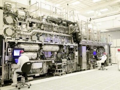
Globalfoundries will make a “multi-billion dollar investment in its Fab 8” to bring up the 7nm process, it said in a press statement.

Globalfoundries picked Everspin’s MRAM as a novel embedded memory, initially for replacing embedded flash in microcontrollers made in its 22nm FD-SOI process. It could also support fast buffers for computer vision chips and eventually be used to replace SRAM in an L3 cache for processors made in its 14nm node.
The density of the embedded offering will vary depending on chip designs, said Gregg Bartlett, head of CMOS products for Globalfoundries. The eMRAM cells sport write speeds “in nanoseconds not microseconds” he said.
The cells require just three masks compared to as many as 13 for embedded flash, enabling reduced space and power consumption. They also sport a thousand-fold improvement in endurance compared to flash, he added.
Globalfoundries has been making 256 Mbit MRAM chips for Everspin in its 300mm Singapore fab for some time. The company holds significant shares in Everspin which is preparing for a public offering, in part to fund design of a Gbit chip.
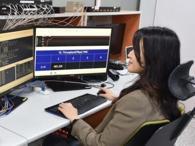
The 22nm FD-SOI process that eMRAM will first be used in currently has 50 customers. First FD-SOI prototypes will move through the fab within a month, said Bartlett.
Jha said Globalfoundries is in no rush to license its unique FD-SOI technology, although one analyst said it could grow the market for FD-SOI with help from Samsung or China fabs.
First products in the 22nm variant won’t ship until early next year and a recently announced 12nm follow-on won’t be ready until 2019. “We are making a market and we want to benefit from that first of all — we are open to [licensing] but we have to make money first,” Jha said.
The company currently has 30 customers with 18 designs running in its Fab 8 on the 14nm FinFET process. They include processors from AMD, IBM’s Power 9 and several ASICs. All are using its second-generation LPP process; only one customer used the early-to-market LPE variant.
Globalfoundries is working on five variations of the FinFET process. They target areas such as delivering highest density, lowest power, high voltage support or automotive requirements.
“We have delivered two 14nm processes and probably will deliver two to four more, but our intention is to not to change the IP but tighten process corners and reduce defects per million,” said Jha.
Globalfoundries made no mention of plans for its 28nm planar process although 28nm is expected to dominate foundry sales for many years. Nor did it describe any new plans for 2.5D or 3D packaging, an area where TSMC has made significant inroads with products such as Nvidia’s Pascal GPU.
The company is ready to support 2.5D and 3D with its 14nm and 7nm nodes, Bartlett said. Before the merger, IBM took an early lead in the area working with Micron on its Hybrid Memory Cube, Patton added.
— Rick Merritt, Silicon Valley Bureau Chief, EE Times
Related links:
Globalfoundries offers embedded MRAM on 22nm FDSOI
TSMC losing market share in foundry ranking
Globalfoundries preps 12nm FDSOI process
Globalfoundries’ CEO on why FD-SOI and why now
 If you enjoyed this article, you will like the following ones: don't miss them by subscribing to :