Imec stacks Gate-all-Around Si nanowires vertically in CMOS MOSFETs
As well as building the GAA nanowire MOSFETs, the researchers also reported their findings on how the intrinsic ESD performance of the MOSFET is impacted by the novel nanowire architecture, proposing the integration of two different ESD protection diodes, a gate-structure defined diode (gated diode) and a shallow-trench isolation defined diode (STI diode).
“GAA nanowire transistors enable ultimate CMOS device scaling, with low degree of added complexity compared to alternative scaling scenarios,” stated Dan Mocuta, Director Logic Device and Integration at imec. The proposed integration scheme for Si GAA CMOS technology and the results on ESD protection are important achievements towards realizing these 7nm and beyond technology nodes. Future work will focus, among others, on further optimizing individual process steps, for example through the co-optimization of the junction and nanowire formation.”

In a horizontal configuration, GAA nanowire transistors are seen as a natural extension of today’s mainstream FinFET technology. In this configuration, the drive current per footprint can be maximized by vertically stacking multiple horizontal nanowires.
Earlier this year, imec scientists demonstrated GAA FETs based on vertically stacked 8nm diameter Si nanowires. These devices showed excellent electrostatic control, but were fabricated for n- and p-FETs separately.
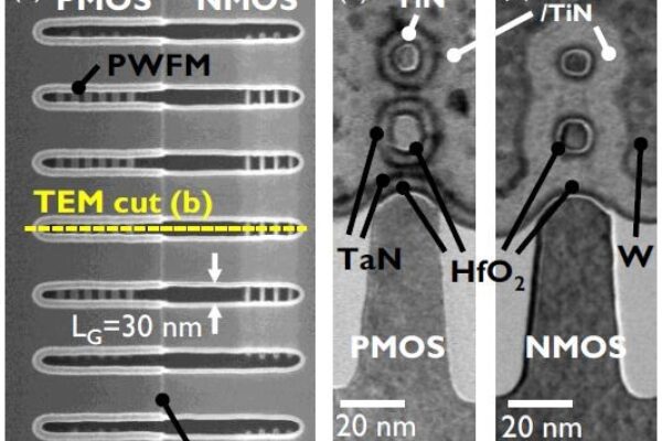
Namely, the two papers presented at IEDM 2016 were: “Vertically stacked gate-all-around Si nanowire CMOS transistors with dual work function metal gates”, and “ESD diodes in a bulk Si gate-all-around vertically stacked horizontal nanowire technology”.
Visit Imec at www.imec.be
Related articles:
Leti’s 5nm node to stack Si nanowires
IMEC reports nanowire FET in ‘vertical’ SRAM
Nanometric transistors take miniaturization into a new dimension
Beyond CMOS: exploring new roads and putting them to work
 If you enjoyed this article, you will like the following ones: don't miss them by subscribing to :