Programmable ASSP interface bridge for mobile image sensors and displays
The company’s CrossLink is a low cost video interface bridge claiming highest bandwidth, lowest power and smallest footprint; is is conceived to resolve interface mismatches between mobile application processors, image sensors and displays. Applications envisaged include VR, drones, cameras, wearable devices, mobile devices and human machine interfaces (HMIs).
The architecture is that of dedicated physical interfaces (transceivers) at the I/O ports of the chip, with a block of OTP (one-time-programmable) FPGA in the centre. You program the FPGA (create the configuration code) in Lattice’s Diamond software; Lattice supplies appropriate functions as importable IP; this IP is provided in source form and is compiled in the Diamond environment, and is there open to customisation. The FPGA ‘core’ usage for typical applications amounts, Lattice has found, to around 2700 to 4300 LUTs. Lattice adds that its highest-growth area is automotive, and the devices are designs to be AECQ 100-qualified, a step which will follow at a later time.
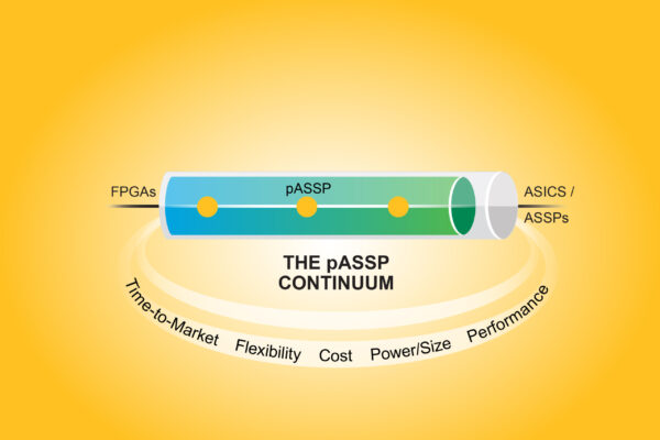
Systems with embedded cameras and displays often, Lattice asserts, do not have the right type or number of interfaces, which can be resolved using a bridge. The CrossLink device combines the flexibility and fast time to market of an FPGA with the power and functional optimization of an ASSP to create a new product class the company calls programmable ASSP (pASSP).
The CrossLink device’s features include:
– Fastest MIPI D-PHY bridging device that delivers up to 4K UHD resolution at 12 Gbps bandwidth.
– Supports popular mobile, camera, display and legacy interfaces such as MIPI D-PHY,
MIPI CSI-2, MIPI DSI, MIPI DPI, CMOS, and SubLVDS, LVDS and others.
– Smallest package size with a 6 mm² option.
– Lowest power programmable bridging solution in active mode.
– Built-in sleep mode.
CrossLink can multiplex, merge and arbitrate between multiple image sensors to a single input. The device can also interface between high-end industrial and popular A/V image sensors with mobile application processors. This is suitable for 360, action, surveillance and DSLR cameras along with drones, and augmented reality products.
With the CrossLink device, it is possible to receive video data from one MIPI DSI interface and send it out over two MIPI DSI interfaces at half the bandwidth. The same video stream can be split to two interfaces, for virtual reality headsets and mobile set top boxes. Designers can also integrate consumer and industrial panels with RGB or LVDS interfaces with mobile applications processors. The CrossLink bridge can convert from MIPI DSI to multiple lanes of CMOS or LVDS interfaces such as MIPI DPI, OpenLDI and proprietary interface formats for HMIs, smart displays, and smart homes.
CrossLink evaluation boards are available from Lattice and its distributors and production devices will be available shortly; www.latticesemi.com/CrossLink
 If you enjoyed this article, you will like the following ones: don't miss them by subscribing to :