Synopsys extends HAPS debug visibility by 100X in FPGA-based prototypes
The new Deep Trace Debug feature enhances both capacity and fault isolation capabilities while freeing up the on chip FPGA memory required for validating complex system on chip (SoC) designs. “The Qualcomm Atheros’ Wi-Fi/Bluetooth combo products use leading edge Wi-Fi standards to achieve gigabit per second throughput, requiring advanced hardware software validation techniques like those available in Synopsys’ HAPS systems,” said Manoj Unnikrishnan, director of engineering at Qualcomm Atheros. “Our traditional approach required multiple runs with a lot of trial and error. The high capacity sample storage available with HAPS Deep Trace Debug allows us to quickly identify bugs and speed full system validation. In addition, HAPS Deep Trace Debug will help us improve state machine coverage, prototyping coverage, and test pattern generation.”
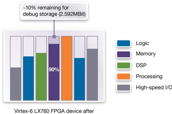
Confirming correct functionality of high speed interface designs often requires sampling at dozens of frequencies for several milliseconds at a time. Traditionally, designers have had to make a choice between capturing long signal trace histories that consume extensive FPGA memory resources or saving FPGA memory resources but losing detailed visibility into signal trace history. By pairing the Synopsys Identify Intelligent Integrated Circuit Emulator (IICE) with a HAPS Deep Trace Debug SRAM daughter board, HAPS Deep Trace Debug allows many unique signal probes with complex triggers to be recorded and provides deeper memory to store extensive state history as the system executes. The SRAM daughter board also frees up the FPGA’s on chip RAM for prototyping an SoC design’s memory blocks.
Visit Synopsys at www.synopsys.com
 If you enjoyed this article, you will like the following ones: don't miss them by subscribing to :