Wafer-level packaging is not enough, say OSATS
The focus of the discussions there was on large format fan-out packaging, or the necessity that OSATS felt, under yield and packaging cost pressures, to move from Fan-Out Wafer-Level-Packaging (FO-WLP) to Fan-Out Panel-Level-Packaging (FO-PLP).
First highlighting the market drivers for FO-WLP, TechSearch International’s president E. Jan Vardaman pointed out how year-on-year mobile devices got thinner and thinner by adopting an increasing number of wafer level packages for their electronic content.
She illustrated this with seven generations of iPhones, thinning from around 12mm to 7mm while increasing their WLP content from 2 dies to over 26 dies.

iPhone Trends: Increasing Number of WLPs. Source: TechSearch International, Inc.
The conventional WLPs trends, she said, include higher I/O counts and larger dies. And together with shrinking geometries, the number of I/Os per die dramatically increased over the years from a few dozens to well over 400, calling for multi-die packages or a move to larger FO-WLP where the I/Os can be distributed not only underneath the die but at the package’s periphery (like extra margins surrounding the die).
Typically, FO-WLP benefit from the same thinness (under 0.4mm) but can integrate multiple dies from different technology nodes, as well as some passives. Nanium offered a good example by moulding together two active dies and 10 surface-mounted passives within a 9x8mm package.

Nanium’s multiple die Fan-Out package integration with passives.
According to TechSearch, FO-WLP could reach over 1.8 billion units per year in 2019, versus less than 300 million packages shipped in 2014. But then, if the trend is to continue, the real-estate on reconstituted wafers will become the limiting factor for optimized larger package integration and cost efficiency, since the piece count remains limited or is even reduced (as the packages grow) on a wafer-like substrate.
As the declining average selling price for end products creates further price pressure, it drives OSATS to develop lower cost package options too, moving to large area packaging beyond today’s wafer sizes. "This is where the wafer fab side, back end assembly, and PCB segments are merging" she said.
Citing a few examples of panel-sized FO-WLP R&D efforts up to 610x457mm2, Vardaman concluded that panel-based processing has a promising future despite the numerous technical challenges it brings with it.
These challenges, just to name a few, include large panel manipulation (new infrastructures moving the dies from wafer-level processing machines to larger panel-capable equipment), die placement accuracy across large panels, panel warpage and new dispensing processes altogether to achieve sufficient molding uniformity and planarity.
Some solutions put forward by Fraunhofer IZM revolve around so-called compression molding, using either a mold-first approach or a redistribution layer-first approach. In principle, it looks fairly simple. A glob of encapsulation compound is poured onto the reconstituted wafer before it is compressed by a panel mould, under vacuum and temperature, until it fills all the interstices between the dies.

Fraunhofer’s molding process, relying on Apic Yamada’s LPM-600 manual (semi-auto) molding system (for panels up to 670x620mm²).
Fraunhofer IZM’s Deputy Group Manager for Assembly and Encapsulation, Tanja Braun discussed her results comparing liquid, granular and sheet lamination molding compounds.
While the paste-like liquid compounds may require complex dispensing patterns to optimize flow, the granular material exhibited the most promising results, as it can be distributed nearly homogeneously all over the cavity before it melts during the compression cycle. It also came out as the most economical with no dispensing limitations for large areas (also faster to dispense than a paste).
When homogeneously spread, the granular material investigated didn’t suffer from the flow marks and knit lines that liquid compounds yielded (regardless of the numerous dispensing patterns investigated).
The lab then went on to mold 250μm thin dies on 610x457mm2 panels (24”x18”) with a mold thickness of 450μm, concluding that although FO-PLP is feasible, there is no simple upscaling of technologies from WL to PL, and new materials will have to be developed in combination with new processes before it can be adopted in volume. Yet, research efforts may be paying back fairly quickly, since moving to large FO-PLP may induce a packaging cost reduction ranging from 20 to 30%, according to the researcher.

Fraunhofer IZM’s FO-PLP results on 610x457mm2 panels.
Rudolph Technologies’ Applications Manager of the Lithography System Group, Roger McCleary was more optimistic about the FO-PLP roadmap, hinting that his company would be ready to support pre-production of large panels as early as 2016, for a full production equipment readiness by 2017 in terms of redistribution layer lithography and the necessary metrology and compensation measures to handle warpage over 5mm.
"There is no long term visibility in the semiconductor back-end industry, yet we expect Fan-Out packages to grow significantly", he said, adding that as the packages get larger, they’ll reduce the piece count on traditional wafers and will push manufacturers to move to larger substrates if they are to achieve a lower cost per package.
McCleary expects the company’s third generation of JetStep lithography equipment to handle panels as large as 650x550mm² (five times the area of a 300mm wafer), delivering a two-fold productivity gain versus 300mm wafer processing on its Stepper. He cited an estimated throughput of 107,113 dies per hour versus today’s 42,504 dies per hour.
Chris Jones, Manager PVD Product Management at SPTS was less upbeat about FO-PLP. "2.5 and 3D die integration in high bandwidth packages is happening now, but when will it move into broader markets?" he asked.
"It’s all about cost, so could FO-WLP fill the gap?"
Jones unveiled some modifications made on the company’s Sigma fxP PVD System to handle 200, 300 and 330mm wafers, but he was keen to point out the resolution and warpage issues of panel-level packaging.
The final speaker, Kevin Yang, Director for Product Management Laser Processing at SUSS MicroTec presented his company’s large format patterning solutions using UV lithography and excimer Laser ablation.
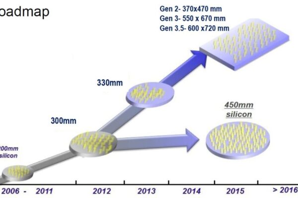
He acknowledged that although all platforms may coexist, the adoption of 450mm wafers was slow, which would probably make panel based packaging a faster growing alternative to reduce packaging costs. Nevertheless, he raised the question of panel standards and infrastructures, what sizes, what materials, what processes and equipment?

A probable FO-WLP roadmap. (source Yole Développement)
He then detailed the specs and promising results obtained using the company’s ELP600, a room-sized excimer ablation system capable of handling substrates as large as 600x600mm.
Related articles:
Nanium takes wafer-level packaging to XXL
TSVs to split more chips: re-integration is the focus
Monolithic 3D integration beats next node
Fan-out wafer level packaging fills gap to 3D, says Yole
 If you enjoyed this article, you will like the following ones: don't miss them by subscribing to :