Peeling electronics off indefinitely re-usable wafers
To achieve defect-free crystalline semiconductor materials on a substrate, epitaxial growth requires a good lattice matching between the substrate material and the new semiconductor layers being grown (for the elaboration of electronic devices). Any mismatch in the materials will yield dislocations and other defects likely to impair the charge mobility and operation of the devices.
Hence, the need to start with bulk wafers of the same material as the one that will be grown on top. But drawing silicon ingots and slicing them into wafers is a costly operation, and exotic materials such as SiC, GaAs, InP or GaP are difficult to grow in large ingots, making the resulting wafers smaller and their use for electronic devices more expensive.
Today’s cost-saving strategy is to slice as many wafers as possible from a given ingot, and then again, most of the substrate material is sacrificed through wafer thinning. Once a device has been grown on top, the reminder of the substrate material merely becomes part of the device’s package (an expensive one in the case of exotic materials).
Publishing their results in Nature under the title “Remote epitaxy through graphene enables two-dimensional material-based layer transfer”, the researchers have used monolayer graphene as a non-stick interfacing sheet between the substrate wafer and the epitaxially grown material.
Through density functional theory calculations, they found that in most cases, a sufficiently thin and electrically penetrable layer of graphene with a weak van der Waals potential would not completely screen the stronger potential field of the underlying substrate, allowing adatoms to experience remote epitaxial registry with the substrate.
Their theoretical calculations indicated that remote epitaxial interactions would be felt through a separation distance up to nine ångströms, a gap large-enough to accommodate a monolayer of graphene.
Experimentally, the researchers confirmed that a monolayer of graphene (even going to four layers) was electrically transparent-enough to allow the adatoms to interact with the underlying substrate, growing a new layer of identical material through so-called remote homoepitaxy.
They applied their new findings to the homoepitaxial growth of GaAs(001) on GaAs(001) substrates through monolayer graphene, explaining that such an approach was also applicable to InP and GaP.

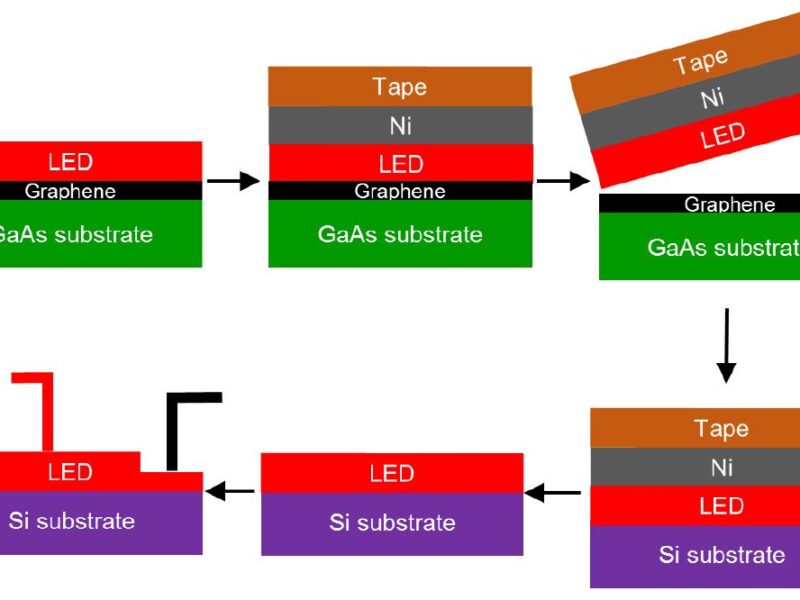
To prove that the newly grown materials were as fit as the bulk substrate to design electronic devices, the researchers grew AlGaInP–GaInP double heterojunction light-emitting diodes (LEDs) on a graphene-overlaid GaAs substrate. The LEDs not only exhibited I–V curves and turn-on voltages (1.3V) comparable to those of LEDs directly grown on a bare GaAs substrate, their electroluminescence spectra also exhibited nearly identical performance.
The LEDs were then exfoliated from the GaAs substrate (leveraging the graphene layer as a non-stick interface from which the active layers could be peeled-off) and transferred to a Si substrate without noticeable performance degradation. The layers being peeled-off are only a few micrometres thick and the graphene-coated wafer remains untouched, ready for re-use without ever being sacrificed in the end-device. That means enormous cost savings, especially so when having to rely on non-silicon substrates.

“Since the epilayers grown by remote homoepitaxy can be released from the graphene surface, this 2D material-based layer transfer (2DLT) technique offers the potential to grow, transfer and stack any electronic and photonic materials on 2D materials without the lattice matching limitation. This will open a pathway towards defect-free hetero-integration of dissimilar materials while saving the cost of expensive and exotic substrates” concludes the paper.

Massachusetts Institute of Technology – www.mit.edu
Related articles:
Slashing costs in 3D IC wafer processing: forget about adhesives!
Developing and strengthening 3D IC manufacture in Europe
Wafer-level packaging is not enough, say OSATS
 If you enjoyed this article, you will like the following ones: don't miss them by subscribing to :