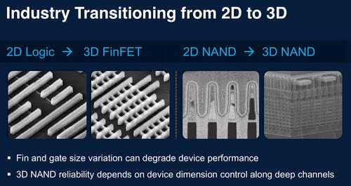
3D E-beam enables 3D NAND Flash
A paper on AM’s technique was presented today at the International Society for Optics and Photonics (SPIE) in San Jose, Calif.
3D NAND flash memory and 3D FinFET transistors have been enabled by critical-dimension scanning electron microscopy (CD-SEM). By applying techniques only recently proven effective in the research lab, AM’s new VeritySEM 5i could not only allow semiconductor makers to speed development of 3D FinFETs but also to finally enable 3D flash memory cubes to be brought to the mass market.
"The industry is transitioning from 2D to 3D," Ofer Adan, global product and technology manager for PDC told EE Times. "So we have the logic guys transitioning to 3D transistors — FinFETS — and the memory guys are transitioning from 2D NAND flash to 3D NAND flash where you stack your NAND device vertically."
The big problem that manufacturers have with FinFETs is turning them all off at precisely the same voltage — the only way you take advantage of the low leakage and subsequent cool running afforded by 3D FinFET transistors.
To control leakage power, you need to control all the different aspects of the 3D gate — the fin height and width, the gate height (sticking out of oxide) and the slope of the gate sides. Unfortunately, none of these parameters can be accurately measured with traditional 2D semiconductor metrology equipment.
The problem with 3D NAND devices is even worse, since the measurements to be made are inside the 3D cube, resulting in only Samsung claiming to be manufacturing devices, and those are not commercially available, but are only being supplied to select cloud customers with no data publicly available on architecture of yields.
"The bottom line is you can not measure 3D devices with 2D metrology and that somebody had to come up with a production worthy high-volume in-line solution for 3D metrology and that’s what we have done."
The main problem for 3D NAND flash, comes after stacking the die when an accurate 60-to-1 high-aspect ratio trench must be etched from top to bottom of the stack, then filled along the edges with oxide-nitride-oxide. Polysilicon put in the middle with tungsten (light blue) forms the flash gate for the memory cells alongside the long trench.
"The big problem with the 3D NAND flash is measuring these 60-to-1 aspect ratio trenches through the stack to the bottom of the trench. Traditional e-beam metrology cannot measure the depth of such a trench," Adan said.
Another problem with high-aspect ratio connections is making sure the long vias bottom-out exactly in the middle of the the copper line they are connecting to (yellow), rather than off to the side. A measurement that is beyond the abilities of 2D metrology equipment, according to Applied Materials.
Both 3D FinFETs and 3D NAND flash cubes are derived from 2D semiconductors, but until now there were no tools to make the critical-dimension scanning electron microscopy (CD-SEM) measurements to get high-yields during mass production. (Source: Applied Materials)
These problems were solved by AM using high-energy electron backscattering, which enables the deep trenches to be accurately measured, resulting in 1.2 nanometer resolution for both the trenches and the accuracy of a vias landing zone, thus allowing the VeritySEM 5i to solve both the research and the high-volume production problems that have been holding back 3D NAND flash memories from mass production and FinFET makers from speeding up development at advanced nodes.
The VeritySEM 5i has already been debugged, and 20 systems are being used by high-profile customers in the field to increase the speed of research and development (R&D) as well as to increase yields on the fab line. Its 1.2 nanometer resolution is already allowing it to be used down to the 10 nanometer node and is expected to work all the way to the 6 nanometer node, according to AM.
About the author:
— R. Colin Johnson, Advanced Technology Editor, EE Times
 If you enjoyed this article, you will like the following ones: don't miss them by subscribing to :