AI, robotics drive GaN power boom
Gallium nitride (GaN) power devices are expanding into various industries, including AI data centres, robotics, electric vehicles, renewable energy, and emerging fields such as digital health and quantum computing, marking a significant increase in the market this year and through to 2030.
In the data centre market particularly, GaN-based power supplies with new topologies are achieving higher efficiencies and power densities than silicon, reducing power losses by up to 30% and enabling the deployment of more efficient and compact data centre architectures. GaN-based motor drives used in humanoid robots can be 40% smaller in size and increase fine movement control.
“If you look at 650V there is not much that is out there in the market,” Dr Johannes Schoiswohl, senior vice president and general manager of the GaN business line at Infineon, tells eeNews Europe.
“We are in the process of working through that and want to release our automotive GaN later this year. At a medium voltage of 100V there is more in the market for LED lighting, audio, also in automotive,” he said.
Market growth
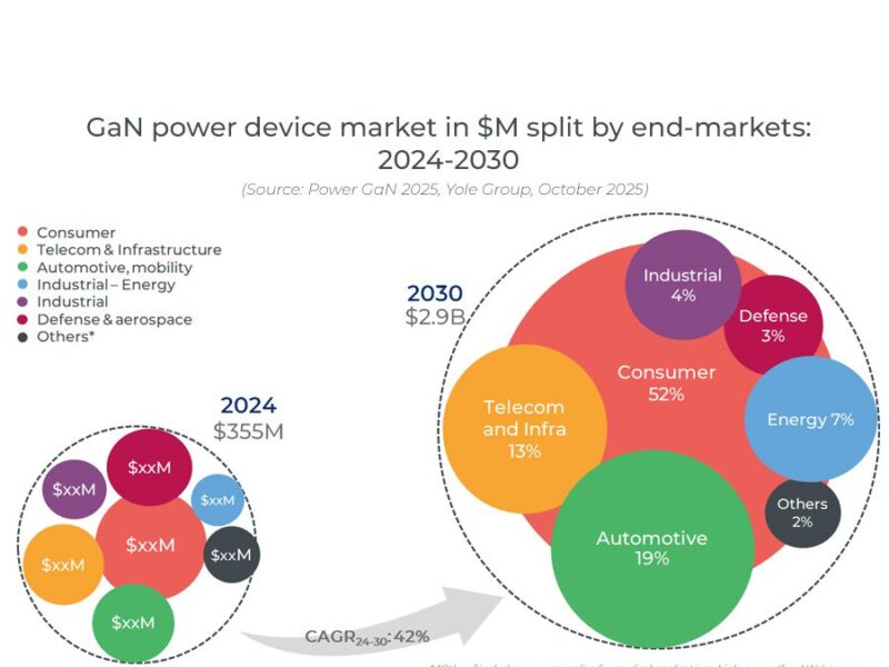
Market analysts at the Yole Group and Trendforce see the GaN power semiconductor market reaching almost $3 billion by 2030, up 400% on 2025. This growth is driven by significant production ramps which began in 2025 across multiple industries, says Infineon. The market for GaN power devices is expected to grow at a compound annual growth rate (CAGR) of 44% from 2025 to 2030, with revenue of $920 million expected in 2026, up 58% on 2025.
Infineon’s high-voltage bidirectional switches (BDS) use a common drain design with a double gate structure with Gate Injection Transistor (GIT) normally off high electron mobility transistor (HEMT) technology rather than a cascode MOSFET design with a Schottky diode. This architecture enables the use of the same drift region to block voltages in both directions, resulting in a significantly reduced die size compared to conventional back-to-back designs. For example, the CoolGaN BDS operates at frequencies up to 1 MHz and provides 40% more power in the same footprint for a solar inverter.
“In the data centre for the 800V to 48V intermediate bus converter (IBC) we see 650 GaN with a stacked topology is the best for power density and efficiency which is critical for the efficiency,” said Schoiswohl. “We see this being picked up by many customers so GaN plays a major role in AI. Then 100V and 80V devices are used for the 48V to 12V conversion and there are also the battery backup units that become higher power in the same space where we see GaN being adopted.”
He points to a three phase Vienna rectifier architecture for power conversion where a 650V bidirectional switch can replace three more expensive SiC MOSFETs with one GaN device, saving system cost.
1200V GaN
Infineon is also pushing to higher voltages above 1000V for solar inverters and transport applications.
“We are getting increasing interest in high voltage GaN at 1200V and we are looking into how such a technology could be established but we are largely following the lateral GaN approach. We see interest in various markets from solar to charge adapters and auxiliary power supplies,” he said.
300mm wafers
The company showed its first 300mm GaN-on-silicon wafer last year and is working with equipment makers to optimise the process for these larger wafers.
The move to 300mm taps into the high volume process technology used for silicon devices to save costs via economies of scale, but is limited by the epitaxial equipment that lays down the GaN layer on a silicon wafer. This equipment, called a reactor, has been optimized for multiple 150 and 200mm wafers and only fits one 300mm wafer.
“We can reduce the cost even considering the different tools,” said Schoiswohl. “That’s a double digit reduction, but halving the cost is not possible and we are working with the tool manufacturers to optimise the tools for a lot lower per die cost,” he said. “We sampled 100V devices late last year and we are on track for the end of this year or early 2027, for production, first with 100V as the epi is thinner so it’s easier to achieve.”
Vertical GaN
Another way to reduce costs is to build vertical rather than planar devices, but this is a challenge for the technology.
“There’s a lot of discussion on vertical GaN but this requires a monolithic GaN wafer which are smaller so today there is a major cost disadvantage. We are assessing the technology but what we see is that GaN on silicon is the better choice. We need to watch that over the next few years but for the voltage range of 650V to 800V this is better, more for 1000V. To be clear, we are not working on a vertical GaN technology, we are doing simulations and watching where it goes,” he said.
The company is also exploring the use of diamond, sapphire and engineered substrates for GaN devices.
A GaN Insights eBook is available here that explores the current state of GaN technology, products, their applications, and the opportunities and challenges that lie ahead.
 If you enjoyed this article, you will like the following ones: don't miss them by subscribing to :