Cadence and partners line up for pre-validated chiplets
Ever wondered what a chiplet is? Think of it as a small, specialised slice of silicon (a “die”) designed to be combined with other dies inside one package, so the finished device behaves like a single big chip. Instead of building a monster monolithic SoC, designers split compute, I/O, memory interfaces and other functions into mix-and-match building blocks, then stitch them together with high-speed die-to-die links. The appeal is better yield, more reuse, and the option to put each function on the process node that suits it best.
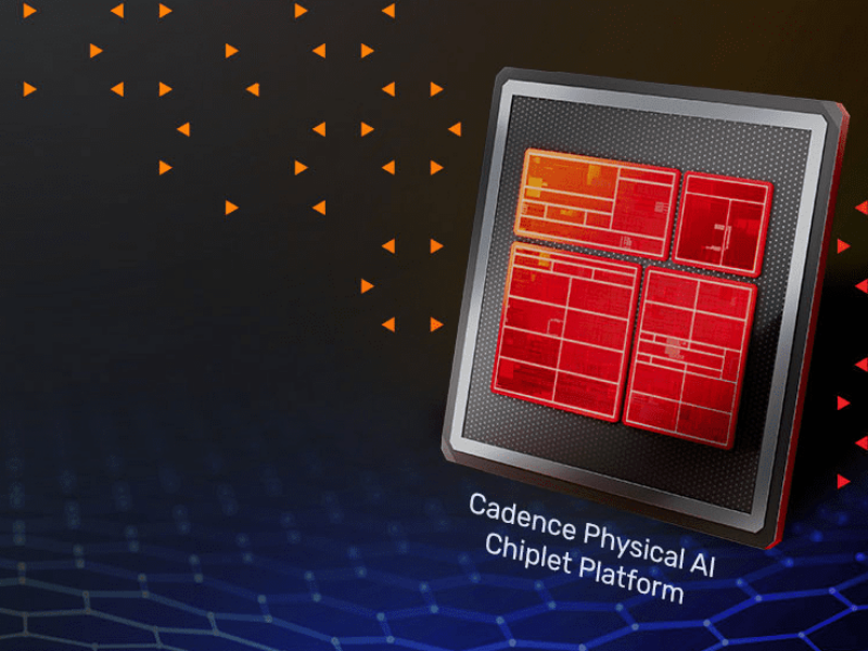
What Cadence is proposing
Cadence is trying to make chiplets less of a bespoke science project by pulling IP partners and packaging know-how into a “spec-to-packaged-parts” flow. The pitch is that you start from a chiplet spec, assemble a framework from Cadence and third-party IP, and then push it through a more repeatable implementation and verification path. Cadence says the target is to reduce integration risk for multi-die designs aimed at “physical AI”, data-centre and HPC workloads.
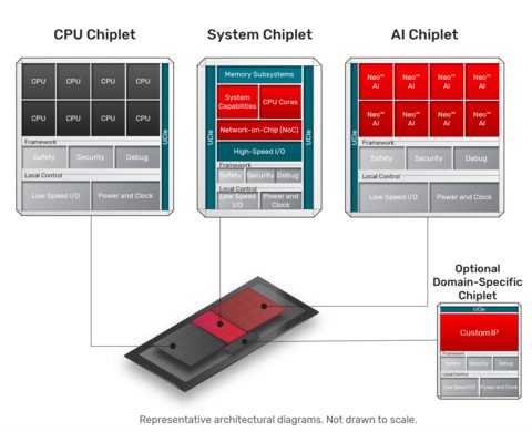
Block diagram illustrating CPU, system and AI chiplets connected as modular dies within a single packaged device, with an optional domain-specific chiplet.
What makes this announcement notable is the emphasis on pre-validated chiplets (and the packaging around them) rather than just “here’s some IP, good luck”. Partners named include Arm, Arteris, eMemory, M31, Silicon Creations, Trilinear Technologies and proteanTecs, alongside a collaboration with Samsung Foundry to build a silicon prototype demonstration on Samsung’s SF5A process. In parallel, Cadence says it will leverage Arm’s Zena compute subsystem and other IP to bolster its chiplet platform and framework.
Why pre-validation matters
The hard part of chiplets isn’t only the individual dies; it’s verifying the behaviour across die-to-die interfaces, package signal integrity, power delivery and thermals, and then doing it again when one block changes. Cadence is positioning pre-validated chiplets as a way to shorten the “unknown unknowns” phase, with flows spanning simulation/emulation and physical implementation. For the underlying announcement details, see Cadence’s partner ecosystem release.
Chiplets are already a live topic on eeNews Europe: Cadence has been active around die-to-die interconnect and tooling, including earlier coverage of its UCIe work here. If Cadence can genuinely turn pre-validated chiplets into something closer to “pick parts, package, verify” rather than “invent your own integration playbook”, that’s a meaningful shift for teams trying to ship multi-die products on a schedule.
 If you enjoyed this article, you will like the following ones: don't miss them by subscribing to :