Can 2D non-volatile memory take on SRAM?
 Cette publication existe aussi en Français
Researchers in China have developed a non-volatile flash memory that can write in just 400ps, substantially less than the time it takes for today’s high speed SRAM memory. But can this take on SRAM in embedded chips?
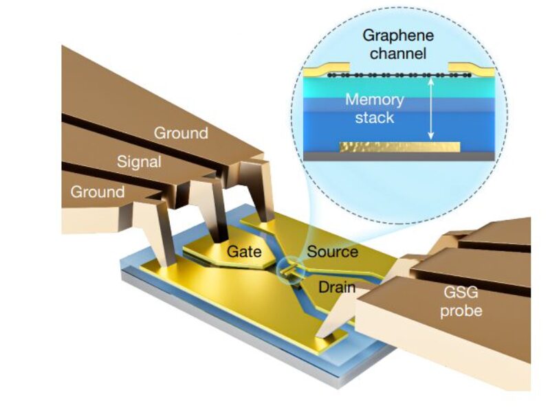
The memory cell developed at the Fudan University in Shanghai uses a 2D structure with either a graphene channel or a tungsten diselenide channel with a hot injection technique.
One of the key questions on using such a structure for memory would be the endurance, especially with the layers that are one atom thick. The team at Fudan report robust endurance over 5.5m cycles, substantially more than silicon-based non-volatile flash. However this is substantially less than SRAM cells, which are typically built with six transistors. In comparison, current embedded ferroelectric FRAM memory calls have an endurance of 1015 cycles.
Extrapolating the data also indicates a storage time of over 10 years for the non-volatile memory.
This is not isolated research. A team at the Department of Materials Science and Metallurgy at the University of Cambridge are working with graphene pioneer Paragraf to developing processes for depositing ferroelectric materials on top of graphene to produce novel memory devices. This could reduce power consumption by about a factor of 10 compared with existing memory device technology.
The 2D Dirac graphene-channel flash memory is based on an enhanced hot-carrier-injection mechanism on a boron nitride hBN/HfO2/Al2O3 memory stack. This supports both electron and hole injection to get the speed of 400ps with a 5V programming voltage. This is faster than an SRAM cell with the same channel length and avoids the need for a charge pump for programming that is needed in a silicon flash memory.
By combining the two-dimensional Dirac band structure and the ballistic transport characteristics, and modulating the Gaussian length of the two-dimensional channel, the researchers realized the super-injection of channel charge into the storage layer.
“The traditional injection behaviour has an injection extreme point, while the super-injection is an infinite injection. The 2D super-injection mechanism pushed the non-volatile memory speed to its theoretical limit, redefining the boundaries of existing storage technologies,” said Liu Chunsen, another researcher on the team.
The next stage is to reduce the length of the graphene channel from 200nm which would provide even faster writing speeds. Improving the endurance would also be a key step to using the technology in embedded chip designs.
 If you enjoyed this article, you will like the following ones: don't miss them by subscribing to :