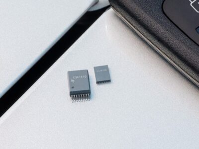
First CMOS UCIe optical chiplet hits 8b Tbps bandwidth
Ayar Labs has announced the first optical interconnect chiplet that adheres to the Universal Chiplet Interconnect Express™ (UCIe™) standard. This optical chiplet aims to maximise AI infrastructure performance and efficiency while reducing latency and power consumption. By incorporating a UCIe electrical interface, the chiplet is designed to eliminate data bottlenecks and integrate seamlessly into customer chip designs.
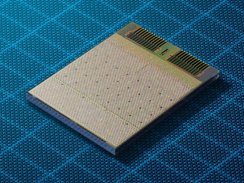
Capable of achieving 8 Tbps bandwidth, the TeraPHY™ optical I/O chiplet is powered by Ayar Labs’ 16-wavelength SuperNova™ light source. The integration of a UCIe interface not only delivers high performance and efficiency but also enables interoperability among chiplets from different vendors. This compatibility with the UCIe standard creates a more accessible and cost-effective ecosystem, streamlining the adoption of advanced optical technologies necessary for scaling AI workloads and overcoming the limitations of traditional copper interconnects.
“Optical interconnects are needed to solve power density challenges in scale-up AI fabrics,” said Mark Wade, CEO and co-founder of Ayar Labs. “We recognized early on the potential for co-packaged optics, which positioned us to drive the adoption of optical solutions in AI applications. As we continue to push the boundaries of optical technologies, we’re also bringing together the supply chain, manufacturing, and testing and validation processes needed for customers to deploy these solutions at scale.”
Ayar Labs has combined silicon photonics with CMOS manufacturing processes to facilitate the use of optical interconnects in a chiplet form factor within multi-chip packages. This enables GPUs and other accelerators to communicate over a broad range of distances, from millimetres to kilometres, while effectively operating as a single, massive GPU.
“The advancement of the UCIe standard marks significant progress toward creating more integrated and efficient AI infrastructure thanks to an ecosystem of interoperable chiplets,” said Dr. Debendra Das Sharma, Chair, UCIe Consortium. “By fostering interoperability and collaboration among vendors, UCIe provides the foundation to meet the growing demands for greater bandwidth and energy efficiency.”
“Co-packaged optical (CPO) chiplets are set to transform the way we address data bottlenecks in large-scale AI computing. The availability of UCIe optical chiplets will foster a strong ecosystem, ultimately driving both broader adoption and continued innovation across the industry,” said Lucas Tsai, Vice President of Business Management at TSMC North America.
“As the industry transitions to a chiplet-based approach to system partitioning, the UCIe interface for chiplet-to-chiplet communication is rapidly becoming a de facto standard,” said Kevin Soukup, senior vice president of GlobalFoundries’ silicon photonics product line. “This accomplishment, uniquely enabled by our monolithic GF Fotonix™ platform, underscores the essential role of silicon photonics in driving highly energy efficient transmission of high-speed data over long distances while maintaining compatibility with chiplet-based standards.”
 If you enjoyed this article, you will like the following ones: don't miss them by subscribing to :