Imec advances 2D-material device technology for future logic scaling
Imec has unveiled two key advances in 2D-material transistor integration at this week’s IEEE International Electron Devices Meeting (IEDM 2025), highlighting record-performing p-type FETs using monolayer WSe₂ and new fab-compatible process modules developed with industry partners. The work strengthens the argument that 2D materials can extend CMOS scaling beyond silicon.
For eeNews Europe readers, the announcement matters because it shows concrete, process-level progress toward manufacturable 2D-FETs—an area closely tied to future logic roadmaps, transistor performance scaling, and Europe’s strategic semiconductor ambitions.
Breakthrough p-type FET integration with WSe₂
While much recent R&D has focused on improving n-type devices based on WS₂ or MoS₂, p-type devices have remained a sticking point. Imec says that is now changing thanks to a collaboration with TSMC that enabled new gate-stack integration techniques for WSe₂ channels.
Gouri Sankar Kar, VP R&D compute and memory device technologies at imec, noted: “At 2025 IEDM, we show in two separate presentations how in-depth collaborations with leading semiconductor manufacturers within imec’s core CMOS Industrial Affiliation Program (IIAP) have enabled breakthroughs in the performance of 2D-material based devices. In both partnerships, combining high-quality 2D material layers provided by the manufacturer with imec’s optimized contact and gate modules played a key role in pushing the technology beyond state of the art.”
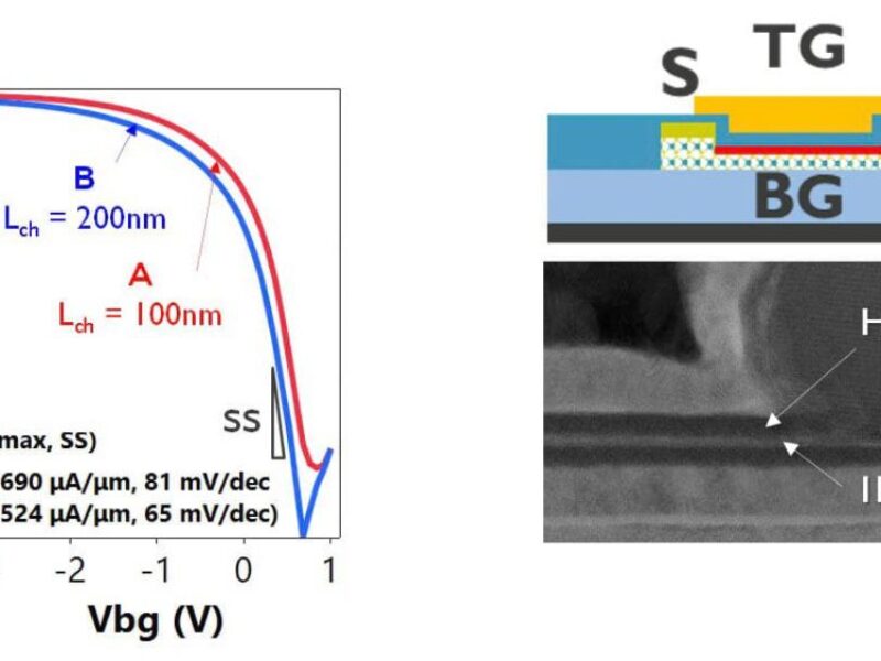
One critical challenge is depositing a top-gate HfO₂ dielectric on MX₂ channels, which typically requires a seed layer. For n-type devices, AlOx works, but WSe₂ behaves differently. Imec and TSMC developed a workaround: a synthetic WSe₂ bilayer made by transferring two monolayers supplied by TSMC, then oxidizing the top layer to create an interfacial oxide that supports HfO₂ nucleation.
According to Kar, “We then oxidized the top WSe2 monolayer, converting it into an interfacial layer that successfully supported the deposition of the HfO2 gate oxide. This fab-compatible lab-based integration approach resulted in record performance of our dual-gated pFETs.”
Intel partnership delivers damascene-style 2D-FET contacts
A second imec presentation describes a collaboration with Intel that targets 300-mm manufacturable process modules for both n- and p-type 2D-FETs. The partners developed a selective oxide etch process applied to Intel’s 2D materials, which were capped with AlOx, HfO₂, and SiO₂ layers.
Kar explained: “The oxide etch process allowed the formation of fab-compatible damascene-style top contacts – a world first. In addition, during the vertical contact etch process, the interfacial AlOx layer was simultaneously etched laterally, removing AlOx from the channel region. This significantly lowered the top gate’s EOT benefiting the gate’s transfer characteristics.”
Imec says the results demonstrate important steps toward viable 2D-material logic integration—particularly in gate stack engineering and contact resistance reduction, two long-standing bottlenecks.
Funding and outlook
Imec’s IIAP Exploratory Logic program and the European 2D-PL pilot line project under Horizon Europe and Horizon 2020 fund this work. As major chipmakers supply industry-grade 2D materials that imec integrates with its process modules, the partners push 2D-FETs steadily closer to real CMOS manufacturing flows.
 If you enjoyed this article, you will like the following ones: don't miss them by subscribing to :