Imec launches 300mm GaN program to drive next-gen power devices
 Cette publication existe aussi en Français
Imec has launched a new open innovation program focused on 300mm GaN technology for both low- and high-voltage power electronics. The initiative aims to advance GaN device performance while cutting manufacturing costs, marking a major step forward for the power semiconductor industry.
For eeNews Europe readers — particularly those in power electronics, semiconductors, and foundry ecosystems — this development highlights a key shift toward 300mm GaN wafer processing that could accelerate GaN adoption in automotive, datacenter, and renewable energy applications.
Expanding GaN to 300mm for performance and cost efficiency
The 300mm GaN program, part of imec’s Industrial Affiliation Program (IIAP) on GaN power electronics, brings together major players AIXTRON, GlobalFoundries, KLA Corporation, Synopsys, and Veeco as the first partners. The collaboration will focus on developing GaN epitaxial growth and high electron mobility transistor (HEMT) process flows compatible with 300mm wafers.
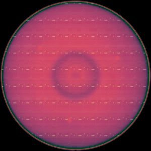
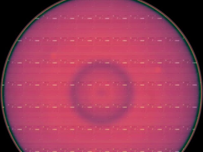
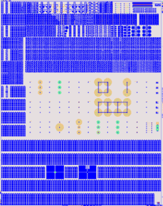
300mm GaN-on-Si wafer from AIXTRON inspected on 8 Series / CIRCLTM tool from KLA Corporation, after p-GaN etch by imec (Source: Imec).
“The benefits of transitioning to 300mm wafers go beyond upscaling production and reducing manufacturing costs,” said Stefaan Decoutere, fellow and program director of imec’s GaN power electronics program. “Our CMOS-compatible GaN technology now has access to 300mm state-of-the-art equipment that will allow us to develop more advanced GaN-based power devices. Examples are aggressively scaled low-voltage p-GaN gate HEMTs for use in point-of-load converters, supporting energy-efficient power distribution for CPUs and GPUs.”
Moving from 200mm to 300mm wafers enables higher throughput, better uniformity, and compatibility with existing CMOS infrastructure — key for lowering costs and enabling integration with other technologies. The new track builds on imec’s 200mm GaN expertise and aims to establish a 300mm baseline platform for both low- and high-voltage applications.
Building the ecosystem for 300mm GaN
Initial work will focus on developing lateral p-GaN HEMT technology on 300mm Si(111) substrates for low-voltage (100 V and above) power devices, addressing process steps such as p-GaN etching and Ohmic contact formation. The next phase targets high-voltage (650 V and beyond) GaN-on-QST® developments using CMOS-compatible engineered substrates with a polycrystalline AlN core.
Meanwhile, control over wafer bow and mechanical strength is a primary concern as the program scales to 300mm. Imec expects to have full 300mm GaN capabilities running in its cleanroom by the end of 2025.
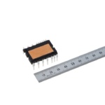
Development mask set for GaN HEMTs on 300mm substrates (Source: Imec).
“The success of the 300mm GaN development also hinges on the ability to establish a robust ecosystem and jointly drive innovation from 300mm GaN growth and process integration to packaging solutions,” added Decoutere. “We are therefore pleased to announce AIXTRON, GlobalFoundries, KLA Corporation, Synopsys, and Veeco as first partners in our open R&D program track on 300mm GaN and hope to welcome more partners soon.”
By bringing together leading equipment and design companies, imec aims to accelerate the transition of GaN power devices toward large-scale, cost-effective manufacturing — paving the way for more efficient, compact, and sustainable electronics across industries.
 If you enjoyed this article, you will like the following ones: don't miss them by subscribing to :