Imec scales solid-state nanopores with EUV lithography
Imec has taken a major step toward bringing solid-state nanopore technology out of the lab and into high-volume manufacturing. At IEDM 2025, the Belgian R&D hub showed the first successful wafer-scale fabrication of solid-state nanopores using extreme ultraviolet (EUV) lithography.
For eeNews Europe readers, this development underlines how leading-edge CMOS processes are finding uses outside mainstream chip scaling. EUV lithography is emerging as an enabler for new device classes, including solid-state biosensors for healthcare applications.
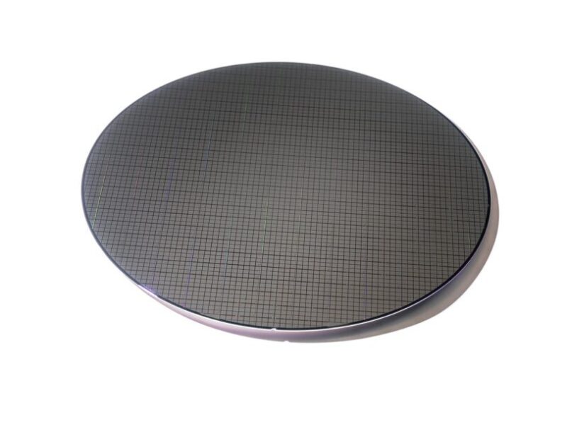
From lab-scale pores to 300mm wafers
Nanopores measure only a few nanometers in diameter, and manufacturers etch them into thin membranes, typically silicon nitride. Applying a voltage across a liquid-immersed membrane causes individual molecules to pass through the pore and generate characteristic electrical signals. This makes nanopores powerful tools for single-molecule detection, including DNA, proteins, and viruses, without the need for labels.
So far, commercial success has mainly come from biological nanopores formed by proteins in lipid membranes. Sequencing platforms use these nanopores, but they face limitations in stability and integration. Solid-state nanopores promise much better robustness, tunability, and compatibility with semiconductor processes, but fabricating them with sufficient precision and uniformity at scale has remained a bottleneck.
Imec’s work tackles that issue head-on. In a paper presented at IEDM 2025, the team reports nanopores with diameters of around 10nm fabricated uniformly across full 300mm wafers. The process combines EUV lithography with a spacer-based etch technique, enabling tight control of pore size and excellent reproducibility.
EUV meets biosensing
After fabrication, imec integrated the nanopores into silicon nitride membranes and electrically characterized them in aqueous environments. DNA translocation experiments confirmed strong signal-to-noise ratios and good wetting behavior, demonstrating that the structures are not just manufacturable but also functional for real biosensing tasks.
“Imec is uniquely positioned to make this leap. We can apply EUV lithography – traditionally reserved for memory and logic – to life sciences. By leveraging our lithography infrastructure, we’ve shown that solid-state nanopores can be fabricated at scale with the precision needed for molecular sensing,” said Ashesh Ray Chaudhuri, first author and R&D project manager at imec. “This opens the door to high-throughput biosensor arrays for healthcare and beyond.”
Toward systems and applications
Looking forward, imec sees applications ranging from rapid diagnostics and personalized medicine to molecular fingerprinting and even data storage. Building on the EUV nanopore process, the institute is developing a modular readout system with scalable fluidics, aimed at helping life science tool developers evaluate chemistry, devices, and system requirements.
Imec is also extending the work into circuit design. At ISSCC 2026, imec will present a 256-channel event-driven ASIC readout for solid-state nanopore sensing. The work shows how advanced electronics tightly integrate with next-generation nanopore arrays.
 If you enjoyed this article, you will like the following ones: don't miss them by subscribing to :