Intel outlines thick-core glass substrate concept for AI data centre packaging
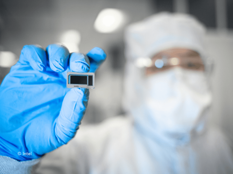
Intel has reportedly showcased a thick-core glass substrate integrated with its EMIB advanced packaging technology, signalling continued development work in glass-based substrates despite earlier uncertainty around its roadmap. The demonstration was said to have taken place at NEPCON Japan, with the technology positioned for high-performance data centre processors.
For eeNews Europe readers working on advanced packaging, heterogeneous integration, or AI accelerator design, the update is relevant as glass substrates are increasingly discussed as a potential enabler for larger package sizes, finer interconnects, and improved mechanical stability in future server-class devices.
Glass substrates and EMIB in advanced packaging
According to Wccftech, Intel Foundry presented a glass-core substrate combined with Embedded Multi-die Interconnect Bridge (EMIB) technology. Glass substrates are being explored across the industry as an alternative to organic materials, potentially allowing tighter line spacing, improved dimensional stability, and reduced warpage at larger package sizes.
In this context, EMIB enables chip-to-chip connections within a single package without requiring a full silicon interposer. The reported combination of EMIB with a glass substrate could therefore support larger multi-die assemblies, which are increasingly relevant for AI and data centre processors that integrate logic, memory, and accelerators within a single package.
The approach reflects broader industry interest in advanced packaging as a scaling path alongside process technology, particularly as AI workloads continue to drive demand for higher bandwidth and increased compute density.
Technical details of the thick-core glass substrate
The reported substrate measures approximately 78 × 77 mm and is described as supporting silicon area equivalent to roughly twice a standard reticle. The structure is said to use a so-called 10-2-10 configuration, with build-up redistribution layers on both sides of a dual-layer glass core.
Ten redistribution layers on the top side are intended to support fine-pitch routing from the attached dies, while a further ten layers on the bottom side help fan out signals towards the package interface. Two EMIB bridges are embedded within the glass core, enabling high-density interconnects between multiple dies inside the same package.
Intel is also reported to have indicated that no significant glass cracking issues were observed during testing, a manufacturing concern often associated with glass substrates due to their brittle nature. If validated at scale, this could be an important factor for server-grade adoption.
Implications for AI data centre processors
While Intel has not announced product timelines, the reported demonstration suggests that glass substrates remain part of its longer-term advanced packaging strategy. For AI data centre applications, such technologies could potentially support larger, more complex multi-die processors while managing mechanical and thermal constraints.
 If you enjoyed this article, you will like the following ones: don't miss them by subscribing to :