Intel to talk of compound FinFET at IEDM
The authorship team will include Welsh wafer supplier IQE plc (Cardiff, Wales). The full program is due to be published towards the end of September.Intel (Santa Clara, Calif.) has caused a stir the semiconductor industry with the introduction of its tri-gate, or FinFET, technology as part of its 22-nm CMOS silicon manufacturing process technology offering.
Intel is the first company to do so with others, such as TSMC and Samsung looking to do so at 14-nm.At IEDM Intel plans to show the way again with a compound semiconductor version that promises faster transistors than silicon. Intel technical executives have in the past tipped InGaAs, possibly embedded on silicon for ease of manufacturing and to carry non-critical circuitry as a way forward for the semiconductor industry. Intel Fellow Paolo Gargini has proposed the integration of an InGaAs quantum-well FET with a high-K dielectric gate stack. (see Intel’s Gargini pushes III-V-on-silicon as 2015 transistor option).
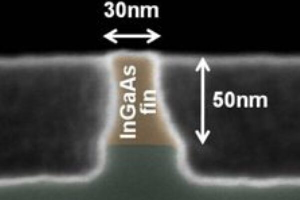
Radosavljevic’s IEDM presentation on InGaAs FinFET devices with improved electrostatic performance, due to the fin shape, looks set to be in-line with that proposal. However, until now, though, the best performing III-V MOSFETs have been planar types, scaled to 10-nm gate lengths and with ultra-thin-bodies.
Two key metrics are sub-threshold slope (the steeper it is, the more abruptly the device can switch) and drain-induced barrier lowering, or DIBL (the smaller it is, the less sensitive the device is to drain voltage and the more efficiently it can turn off). Long-channel devices exhibited a subthreshold slope of 66 mV/decade, close to the theoretical minimum of 60 mV/decade, while DIBL of short gate length devices was significantly improved over best-in-class planar III-V MOS devices. The better electrostatics of these devices comes from their narrow fin width and high-quality high-k gate dielectric.

 If you enjoyed this article, you will like the following ones: don't miss them by subscribing to :