Manufacturers’ top tips to cost-effective 3D IC production
One of the big questions at Grenoble’s 3D TSV Summit was: how to distribute the cost-of-ownership across the supply chain?
Who should manufacture TSVs?
In non-MEMS ICs, TSVs must shrink too, because going to the next generation node does not necessarily make sense if your TSV keep-out zone takes too much premium silicon. The processes require equipment sets typically seen in wafer fabs, hence TSV integration could be done by the foundries, but also to some extent by OSAT service providers (Outsourced Semiconductor Assembly and Test). Some printed circuit board (PCB) makers are also looking at embedded dies into PCB substrates, in the form of active interposers for 2.5D integration.
Putting aside the current economic climate which could limit TSV ramp up in the near term, Gartner’s Mark Stromberg expects the TSV market to faces capital cost issues that will limit the number of companies able to implement this technology. This is due mainly to the additional capital and material costs, together with more process steps. “As we move to the 10nm node, TSV technology will be require for system design”, Stromberg said, noting that the cap-ex requirements will reduce competition with only the top Integrated Device Manufacturers (IDMs), foundries and top tier Semiconductor Assembly and Test Services (SATS) able to compete.
Dr. Miekei Ieong, Vice President of TSMC EMEA, presented his company’s CoWoS (Chip-on-Wafer-on-Substrate) services relying on through silicon via technology to integrate multiple chips into one single package using a submicron scale silicon interposer. The company offers homogeneous CoWoS in production but says it has already demonstrated heterogeneous CoWoS. A 512-bit Wide I/O DRAM test chip was operated at 200MHz and even overdriven up to 285MHz with full operations.

“Our 1024-bit TSMC CoWoS DRAM was driven to 1GHz, supporting a bandwidth up to 128GB/s”, said Ieong, with plans to tape-out daisy-chained 6 top dices high bandwidth memory by the last quarter of this year.
For the purpose of larger CoWoS, TSMC has also demonstrated silicon interposers up to 26x48mm on a substrate size of 60x60mm. The company says it is ready for stacking memory chips on 28nm logic, and it has characterized TSV design rules for customer’s test vehicle design and functional verification.
Global Foundries’ Michael Thiele, Responsible for Packaging R&D, exposed his company’s readiness with TSV-capable lines installed in Malta, New York, with TSV integration characterized for 20nm devices and 14nm under way. The company has a 300mm TSV line installed in Singapore for Si interposer fabrication and is characterizing TSV integration into 28nm devices in Dresden, Germany.
“Before considering a 2.5D product tape-out, customers expect the foundry to come up with system level qualification data from a representative test vehicle”, stated Thiele who then unveiled Global Foundries’ dual approach, using external test vehicles with shared R&D but also creating its own internal test vehicle.
Hence, the company develops interposers and micro-pillar interconnects both at OSAT partners and in-house. But Thiele stressed that yield loss, late in the supply chain, could stop the adoption of the technology, especially if there is not a clear yield ownership in the supply chain. Cost reduction at key process steps such as TSV drill and fill, temporary wafer bonding and de-bonding, TSV reveal, is another must for 3D ICs to make it to the mass market.
Cutting on materials and process costs
Director for Industry Development at the A-star Institute of Microelectronics (IME), Surya Bhattacharya sees back-end of line (BEOL) and thin wafer handling (including temporary wafer bonding and de-bonding – TBDB) as a real cost-issue for 3D IC components. These added processes alone amount to around 50% of the total final component cost, he estimates.
Bhattacharya’s drastic cost-cutting approach is to rely on low-cost multi-level copper redistribution layers (Cu RDL) in thick photo-dielectrics (polymers), requiring fewer processing steps, no CMP steps and no dielectric etch. The lab has developed photoresist materials and has demonstrated Cu RDL fabrication for different line widths and spacing, at 5/5µm and 3/3µm, with three levels of metal.
The copper redistribution layer with a line width of 3um and a polymer pitch of 6um was demonstrated to support 20Gbit/s signals across a 10mm interconnect, versus 7.5Gbit/s for the costlier 1um wide copper line in a damascene structure, at a 4um pitch. The lab is also experimenting with 2um thin copper lines in polymer, and targets 0.5µm line width by 2016 to stay competitive with very fine TSVs.
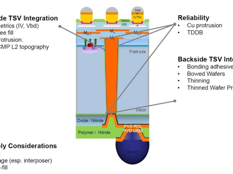
On top of this approach, Bhattacharya exposed a carrier-less technique to avoid or reduce the TBDB steps, whereby after chip-to-wafer bonding and underfilling, the full wafer is over moulded and flipped for backside via reveal, directly maintained by the epoxy mould compound.

IME’s carrier-less process flow using wafer-level over molding.
Altogether, removing the back end of line (BEOL) Cu RDL deposition processes and the TBDB steps, Bhattacharya roughly estimates that wafer-level processing costs could be slashed by 40% to 50%.
“Moving from a copper and damascene structure to a copper redistribution layer into an organic layer can cut 15 to 20% of your processing costs” concurred Sesh Ramaswami, Managing Director for Packaging Technologies and Advanced Product Technology Development for the Silicon Systems Group at Applied Materials.
One way to reduce the lengthy and costly CMP process is to fine tune the growth of the via and the subsequent via reveal step so as to stop the etch right when the vias are revealed, with only little material to remove during the Chemical Mechanical Planarization to open the vias and trim them down to the wafer surface.
Director of Process Technology at Tel Nexx, Steve Golovato exposed a cost of ownership analysis for high aspect ratio TSVs built up using conformal barrier-seed deposition. Using this particular TSV filling, Golovato says the industry could contain CMP costs compared to using Ionized PVD barrier-seed deposition which can create a material overburden atop the via (and requires more CMP to be removed).

More interestingly, Golovato expects his company’s electroless Cu conformal barrier-seed deposition technique to be up to 50% lower cost than I-PVD for TSVs with an aspect ratio of 20, at wafer-level.
Precise via reveal
Vice President of Marketing at SPTS, David Butler aims to minimize the CMP step by optimizing the via reveal step. SPTS has developed Deep Reactive-Ion Etching (DRIE) equipment capable of etching at rates up to 4.7um/mn (with a uniformity of ±3.0%). That is twice as fast as competitors, according to Butler, and up to four times faster than wet-etch approaches. Another important advance is SPTS’s ReVia in-situ end-point detection. Based on IR interferometry, this automated optical analysis feature looks at groups of vias across the surface being etched and is able stop the via-reveal process when via tips emerge, only 1um above the surface.

SPTS’s ReVia in-situ end-point detection yields via tips only 1µm above the wafer surface
This avoids costly rework operations, typically more etch if not all the vias are revealed, or yield issues if the wafer is etched beyond usability. The company also implements dual source tuning for etching, which allows its equipment to tightly control etching across the wafer, radially. This can be used to compensate for wafer thickness variations after the wafer thinning step. Last, the company introduced its Rapier XE, its next generation equipment capable of etch rates up to 9um/mn entirely tuneable radially and promising four fold productivity gains.
Related articles:
3D IC ramp up: what can we learn from MEMS?
Developing and strengthening 3D IC manufacture in Europe
Slashing costs in 3D IC wafer processing: forget about adhesives!
Automated design-for-test solution for 3D memory-on-logic
 If you enjoyed this article, you will like the following ones: don't miss them by subscribing to :