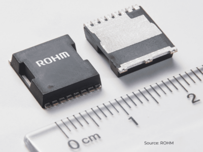
Next-gen GaN transistors come in sight, targeting electromobility
Within the scope of the ZuGaNG project, the Fraunhofer IAF scientists are digging deeply into the research GaN matter. The improved technology they are preparing promises higher switching speeds, which would translate into higher energy efficiency for the voltage converters in which they are used. Besides higher efficiency, the technology also holds out the prospect of reducing manufacturing costs significantly; the institute believes that the savings could sum up to 50%, compared to today’s GaN devices.
Physical characteristics of Gallium Nitride such as high electron mobility and high critical field strength enable the design of transistors with higher durability and robustness than their conventional silicon counterparts. The high switching frequency in addition makes it possible to reduce the space requirements since the passive components can be smaller. "The miniaturisation allows us to reduce the cooling requirements and the volume which in turn translates into lower manufacturing and operating cost", explains Fraunhofer project manager Patrick Waltereit.
The research includes new concepts for semiconductor design, materials production, and process technology for the production of GaN power devices. Soon, demonstrators will be available to prove the performance of DC/DC converters utilising these next-gen GaN transistors; application fields include electromobility, battery chargers for electric cars as well as industrial manufacturing, home appliances, and photovoltaics. As one particular application in manufacturing technology, the researchers highlight generators for plasma and laser systems.

Almost ready: Demonstrator for the next generation of Gallium Nitride power semiconductors. (Source: Fraunhofer IAF)
Besides developing these demonstrators, the researchers will provide a comprehensive characterisation of GaN transistors to achieve a thorough understanding of the correlation between manufacturing parameters on one side and the structural, electrical and thermal properties of GaN devices on the other side. In addition, the technology will be optimised for reliability and robustness to qualify it for industrial deployment.
One innovative approach to reduce manufacturing costs for GaN transistors targets designs that can be executed on standard CMOS production lines. In addition, the project intends to combine the specific integration potential, the high throughput and the excellent functionality of the CMOS technology with the high power density and robustness of GaN components to tap the promising potential of optimised power electronics.
Participants of the ZuGaNG projects are, besides Fraunhofer IAF, a number of commercial companies that cover the entire value chain for the future product generation, including Robert Bosch GmbH, laser tool manufacturer Trumpf, semiconductor foundry X-Fab, as well as a number of universities. The project is partly founded by the German federal research ministry BMBF with 3 million euros.
Related articles and links:
Market for GaN and SiC power semiconductors set to rise by factor of 18 in next decade
Audi, Bosch get granular on GaN
 If you enjoyed this article, you will like the following ones: don't miss them by subscribing to :
eeNews on Google News


