
Power innovations drive AI rack development
Rapid advancements in AI hardware are dramatically increasing both power consumption and density within data centres. In just a few years, the power requirements of AI accelerators have surged from 100W to over 1000W, pushing rack-level demands from 20 to 30kW to more than 100kW, with projections reaching up to 500 kW in the near future. Under these conditions, conventional power supply methods are approaching their physical and operational limits.
This is driving new power conversion architectures at higher voltages of 800V across many companies, driven by new open source rack architectures developed by Nvidia.
There is a commercial imperative as well. “By moving power conversion upstream we simplify the entire system and allow us to have more performance per watt and more GPUs per AI factory,” says Joe DeLeare, who is respomsible for datacentre product marketing at Nvidia.
There are many different techniques being developed to provide the power conversion, from sapphire-based high voltage 1250V gallium nitride (GaN) from Power Integrations to combinations of GaN and silicon carbide (SiC) from Rohm and Infineon Technologies. Many power device suppliers are offering a range of device technologies and topologies to address the opportunity in billions of dollars of AI factory roll outs.
Current AI systems combine four power conversion stages, from the AC mains down to the core voltage, in the same rack as the GPUs and CPUs. The first two, AC to 400 VDC and 400 VDC to 54 VDC are grouped in power supply units, and along with battery backup units, located in dedicated power shelves. From there, the 54 VDC is distributed down the rack to the compute trays or shelves, where the last two stages convert the 54 VDC into 12 VDC, and finally the 12 VDC into the core voltage.
“Given rapid growth in the server and artificial intelligence (AI) markets, the amount of energy required per rack is increasing from 100kW to over 1MW. This increase requires designers to fundamentally reimagine the entire data centre’s power delivery path, from the grid to the gates of processors,“ says Jeff Morroni, chief technology officer of power at Texas Instruments. “Using 48V distribution with a 1MW rack would require almost 450lbs of copper to maintain distribution losses – an unsustainable amount in both weight and cost. That’s why we’re working with Nvidia to codevelop an 800V high-voltage DC distribution ecosystem to enable further scaling of computing needs and power.”
The rapid rise in power consumption of high-performance AI servers—particularly GPUs—is driving a fundamental rethinking of data centre power delivery. Traditional multi-stage conversion systems incur substantial energy losses, making efficient power delivery increasingly challenging.
With 800 VDC, the same wire gauge can carry 157% more power than 415 VAC. Using a simpler three-wire setup (POS, RTN, PE) instead of four for AC, fewer conductors and smaller connectors are required. This reduces copper use, lowers material and installation costs, and eases cable management, critical as rack power inlets scale toward megawatt levels.
A native DC architecture eliminates multiple, inefficient AC-to-DC conversion steps that occur in traditional systems, where end-to-end efficiency can be less than 90%. This streamlined power path boosts efficiency and reduces waste heat.
The traditional centralized PSU is restructured with different conversion topologies. The ACDC conversion stage is relocated to a side-rack power source, where efficiency optimization is critical The DC-DC stage remains within the IT rack, where maximizing power density is essential to free usable board area.
Based on internal analysis, Rohm sees the optimal configuration is achieved by using SiC devices in the power source stage and GaN devices in the AI rack.
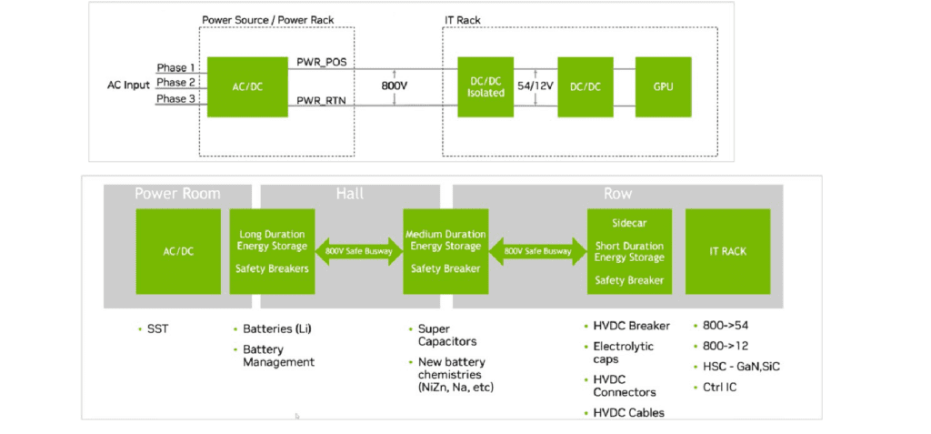
The power conversion architecture in AI racks Courtesy of Rohm
Existing AC-DC converters typically target the 20kW to 33kW range, with output power levels expected to scale even higher. For 800VDC systems, Rohm recommends an optimal AC-DC topology that combines a Vienna Rectifier PFC with a three-phase isolated LLC converter
The power source consists of a Vienna rectifier that converts three-phase 400VAC to 800VAC, followed by an LLC converter for galvanically isolated 800VDC output. High efficiency is paramount for this stage.
The diodes used in Vienna rectifiers require 1200V rating and excellent recovery characteristics, making SiC SBDs the ideal choice. Unlike Si FRDs, SiC SBDs are unipolar and do not accumulate minority carriers, eliminating recovery loss.
For the bidirectional switches, back-to-back devices rated at 650V or higher are typically used. This configuration doubles the conduction resistance, making low on-resistance, fast-switching characteristics essential. Rohm’s 750V-rated SiC MOSFETs meet these requirements, combining a low on-resistance for higher speed switching.
Rohm also points to its DOT-247 package that integrates two SiC MOSFETs in a common-source configuration. The optimized design reduces parasitic inductance, enabling high-speed switching while contributing to miniaturization by requiring fewer components than conventional discrete implementations.
Simulation results using the Rohm PLECS tool for the conversion efficiency and power loss in the Vienna rectifier account for power device losses but exclude peripheral components such as reactors and capacitors. The results demonstrate a conversion efficiency exceeding 99% at up to 50kW.
Operating in a three-level configuration, the rectifier applies only half the voltage to switching devices compared to a conventional two-level PWM rectifier. This reduces switching losses and enables the use of lower-Ron, lower-voltage components for improved efficiency. Additionally, the three-level operation produces smaller voltage changes across the inductor, leading to lower ripple current and reduced noise.
Direct conversion
To provide megawatt power, EPC in the US has developed a low-cost, low-profile GaN-based, 6 kW 800 V-to-12.5 V converter based on an Input Series Output Parallel (ISOP) topology.
The design occupies under 5,000 mm2 and only 8 mm in height, making it ideal for space-constrained AI boards. It also converts 800 VDC to 12.5 VDC close to the load, reducing bussing losses and improving system-level efficiency.
By moving from AC directly to 800 VDC at the rack level, and then stepping down to 12.5 V at the board, the GaN-based ISOP topology eliminates unnecessary conversion stages and enables the scalability, simplicity, and energy optimization demanded by tomorrow’s AI data centres.
“GaN is an essential technology for the 800 VDC ecosystem,” said Alex Lidow, CEO of EPC. “Our collaboration with Nvidia is to develop compact, efficient, cost-effective board-level conversion to power future AI factories at gigawatt scale.”
The 6 kW 800 VDC to 12.5 V ISOP converter supports 800 VDC power distribution in AI infrastructure by using an LLC topology in an input-series, output-parallel (ISOP) configuration [1]. This configuration uses a modular approach where the input voltage and output current are divided over eight blocks, where each block only experiences 1/8th of the input voltage and produces 1/8th of the output current. As a result, the original converter specification of 800 VDC to 12 VDC (64:1 conversion ratio) is reduced to a much simpler 100 VDC to 12.5 VDC (8:1 ratio) with 750 W output power rating for each module.
Each module is configured with a half-bridge input and centre tap output transformer with a turns ratio of 4:1:1. This transformer is cost effective because it is easily constructed as a planar transformer with the windings integrated into a PCB. The centre tap secondary has the additional benefit of requiring only a single FET in the high-current path as opposed to two in series when using a full-bridge rectifier.
The elegance of this design is in its simplicity. The LLC modules are designed to operate at the resonant frequency, where efficiency is the highest and the gain of the resonant tank is unity. The gain of the converter remains frequency independent around the operating frequency and over a wide range. This forces the parallel outputs to present equal voltages to each of the primaries, including, component tolerances to maintain equally divided voltages across each of the modules. Since all inputs are in series, the current through each input is identical, balancing the current on each of the outputs.
With zero-voltage, zero-current switching of the LLC, these low voltage modules are very efficient, even at high frequencies. EPC’s embodiment of this solution has each module switching at 1 MHz, which enables the low-profile core height of under 8 mm. This height is critical as it allows many AI boards to be stacked in the rack without disrupting the cooling of the processors.
1250V GaN
Power Integrations (PI) is aiming its automotive-qualified sapphire=based GaN chips at the AI rack application.
“There is a convergence of automotive with datacentre at the higher voltages,” said Chris Lee, director of product marketing at PI. “We have a unique position with the quality from automotive and multiple high volume platforms for automotive supply chains which is also important.”
“We have our own epi process and we use standard foundry services so we control process. We have our GaN on sapphire and use silicon foundries and we have been in extremely high volume applications. We build the devices on 6in sapphire wafers with multiple foundries and multiple fabs in Japan and we do have a foundry partner in the US that is capable of the final stages,” he said.
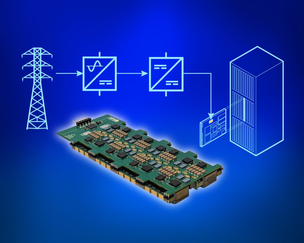
EPC is proposing an ISOP topology for 800V direct conversion Source EPC
“Our 1250V GaN simplifies the topology with a single half bridge to achieve a higher density for 800V to 12V which is what the architecture is looking for,” he said, “This also allows higher frequency targeting 1MHz – we want to push the frequency as high as we can and 1MHz offers the best balance of switching noise and EMI noise – moving beyond that frequency introduces other challenges.”
PI introduced its 1250V cascode GaN device in 2023 that has since been qualified for automotive and a 1700V device in 2024. “We are not finished and we still have a high confidence that we will bring the technology to the next level with the option to replace SiC,” said Jimmy Liu, director of product definition at PI.
The higher voltage is achieved with a cascode design with a low voltage silicon MOSFET mounted on the GaN transistor in the package to reduce the parasitic signals. PI also makes the LV silicon MOSFET with lower RDSon typically single ohm and 30 to 40V breakdown voltage and this makes the GaN device easier to drive.
“We are hearing about a 600kW and 1MW rack and without this technology it will be very difficult to achieve these power levels,” said Lee. “What we are working on is to define the final product that will use the 1250V device for the half bridge and full bridge topologies to tackle the main power conversion for the driver and the package using existing technology. We are talking to the ODMs in Taiwan and the US about to help them with the technology and a reference design is an excellent vehicle for that.”
“With the growth of AI, data centres are evolving from simple server rooms to highly sophisticated power infrastructure hubs,” said Chris Suchoski, sector general manager, Data Centers at TI. “Scalable power infrastructure and increased power efficiency are essential to meet these demands and drive future innovation. With devices from TI, designers can build innovative, next-generation solutions that are enabling the transition to 800 VDC.”
Future direction
The 800V architecture will be used in the Nvidia Kyber rack architecture where the power is distributed at a high voltage directly to each compute node, where a late-stage, high-ratio 64:1 LLC converter efficiently steps it down to 12 VDC immediately adjacent to the GPU. This single-stage conversion is more efficient and occupies 26% less area than traditional multi-stage approaches, freeing up valuable real estate near the processor.
Future AI racks proposed by Nvidia Source Nvidia
However this needs a fundamental change to the design of the racks and boards in the AI datacentre. This includes a liquid cooled bus bar that can handle the incoming currents at 800V and distribute this to the GPUs. Nvidia will not currently comment on this technology. “The liquid cooled busbar is new and the plan is to contribute that to the open source community,” said DeLeare
The innovations are not just in the power devices. Nvidia is also adding new components such as supercapacitors into the rack to smooth out the peaks and troughs of the power delivery. “The supercapacitors allow us to smooth the spikes from the grid and this can save up to 30% in the peak power required by the datacentre,” he added.
www.nvidia.com; www.power.com; www.ti.com; www.rohm.com; www.epc.co; www.infineon.com;
 If you enjoyed this article, you will like the following ones: don't miss them by subscribing to :