Rapidus selects Hokkaido for 2nm wafer fab site
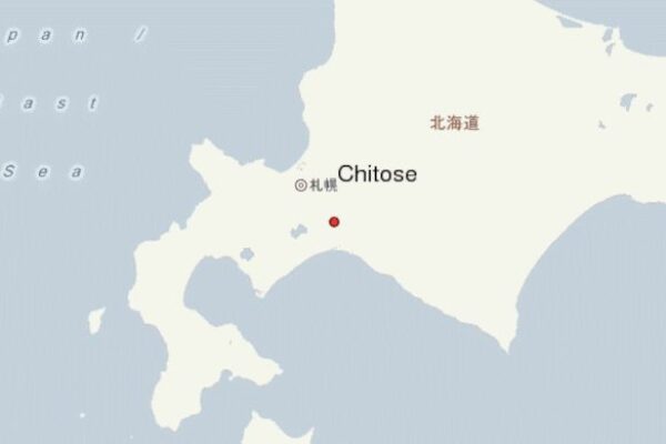
Rapidus Co. Ltd. (Tokyo, Japan), the newly-formed logic foundry aiming at 2nm production, has selected Chitose City, on the northern island of Hokkaido, as the location for its wafer fab.
The company, which is in partnership with IBM and IMEC to further develop the node, expects the factory to host a prototype line in 2025 and enter mass production in the late 2020s. The project is expected to cost as much as 5 trillion yen (about US$37 billion).
“Chitose City in Hokkaido is ideal for semiconductor production in terms of its harmony with the natural environment, in addition to infrastructure such as water and electricity,” said Atsuyoshi Koike, in a statement.
Observers have pointed out that Hokkaido is not a major semiconductor hub and lacks a supply chain for chip production. The Rapidus project will therefore need to stimulate investment by semiconductor ecosystem companies, including chip equipment makers and material suppliers.
“We chose this location as the planned site for our factory because of its medium- to long-term potential, such as global personnel exchanges and the development of an ecosystem. In the future, after the government approves the plan and budget, we would like to start concrete discussions with Chitose City,” said Koike.
Related links and articles:
News articles:
Rapidus seeks billions of dollars to use IBM’s 2nm process
Consortium forms Rapidus to get Japan back into chip race at 2nm
Japan’s Rapidus signs up IMEC to support 2nm push
Japan budgets $2.4 billion for chip R&D hub with US, Europe
Japan, US make plans for independent 2nm production
IBM announces 2nm chip, and manufacturing process
 If you enjoyed this article, you will like the following ones: don't miss them by subscribing to :