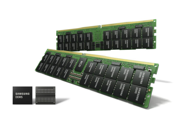
Samsung starts mass production of 14nm EUV DDR5 DRAM
Samsung Electronics has started mass production of its 14nm DDR5 DRAM memory devices based on extreme ultraviolet (EUV) technology.
“We have led the DRAM market for nearly three decades by pioneering key patterning technology innovations,” said Jooyoung Lee, senior vice president and head of DRAM Product & Technology at Samsung Electronics. “Today, Samsung is setting another technology milestone with multi-layer EUV that has enabled extreme miniaturization at 14nm — a feat not possible with the conventional argon fluoride (ArF) process. Building on this advancement, we will continue to provide the most differentiated memory solutions by fully addressing the need for greater performance and capacity in the data-driven world of 5G, AI and the metaverse.”
By applying five EUV layers to its 14nm DRAM, Samsung says it has achieved its highest bit density while enhancing the overall wafer productivity by approximately 20 percent. The 14nm process can help bring down power consumption by nearly 20 percent compared to the previous-generation DRAM node.
The DDR5 standard enables data transfer speeds of up to 7.2 Gbit/s, twice that of DDR4.
Samsung plans to expand its 14nm DDR5 portfolio to support data centre, supercomputer and enterprise server applications and grow its 14nm DRAM chip density to 24Gbit.
The company is also using a 10nm-class EUV process for DDR5 memories that extends to 32Gbit devices with a 30 percent power reduction.
Related articles
- First open-source software kit for CXL memory
- Samsung looks to 2nm in 2025
- Samsung ups foundry prices to fund capacity expansion
- Samsung backs off from NXP deal
- Samsung to build 3nm US fab
Other articles on eeNews Europe
- Opinion: Politicising semiconductor manufacturing is a global failure
- US summit on quantum industry highlights skills shortage
- Sysgo updates PikeOS for space
- ZF, Oxbotica team for driverless shuttles
- NXP strips down i.MX 8XLite for secure industrial IoT
- Intel backs RISC-V for Nios FPGA processor
- European supercomputer project receives RISC-V test chips
 If you enjoyed this article, you will like the following ones: don't miss them by subscribing to :