Single atom thin semiconductors enable flexible devices
At issue are molybdenum sulfide (MoS2) thin films that are only one atom thick, first developed by Dr. Linyou Cao, an assistant professor of materials science and engineering at NC State. MoS2 is an inexpensive semiconductor material with electronic and optical properties similar to materials already used in the semiconductor industry.
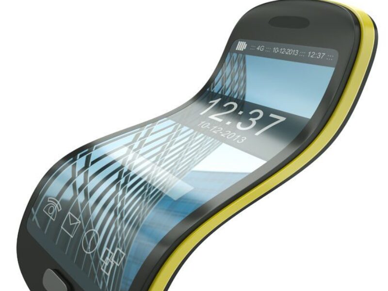
"The ultimate goal is to use these atomic-layer semiconducting thin films to create devices that are extremely flexible, but to do that we need to transfer the thin films from the substrate we used to make it to a flexible substrate," says Cao, who is senior author of a paper on the new transfer technique. "You can’t make the thin film on a flexible substrate because flexible substrates can’t withstand the high temperatures you need to make the thin film."
Cao’s team makes MoS2 films that are an atom thick and up to 5 centimeters in diameter. The researchers needed to find a way to move that thin film without wrinkling or cracking it, which is challenging due to the film’s extreme delicacy.
"To put that challenge in perspective, an atom-thick thin film that is 5 centimeters wide is equivalent to a piece of paper that is as wide as a large city," Cao said. "Our goal is to transfer that big, thin paper from one city to another without causing any damage or wrinkles."
Existing techniques for transferring such thin films from a substrate rely on a process called chemical etching, but the chemicals involved in that process can damage or contaminate the film. Cao’s team has developed a technique that takes advantage of the MoS2‘s physical properties to transfer the thin film using only room-temperature water, a tissue and a pair of tweezers.
MoS2 is hydrophobic – it repels water. But the sapphire substrate the thin film is grown on is hydrophilic – it attracts water. Cao’s new transfer technique works by applying a drop of water to the thin film and then poking the edge of the film with tweezers or a scalpel so that the water can begin to penetrate between the MoS2 and the sapphire. Once it has begun to penetrate, the water pushes into the gap, floating the thin film on top. The researchers use a tissue to soak up the water and then lift the thin film with tweezers and place it on a flexible substrate. The whole process takes a couple of minutes. Chemical etching takes hours.
"The water breaks the adhesion between the substrate and the thin film – but it’s important to remove the water before moving the film," Cao says. "Otherwise, capillary action would case the film to buckle or fold when you pick it up.
"This new transfer technique gets us one step closer to using MoS2 to create flexible computers," Cao adds. "We are currently in the process of developing devices that use this technology."
Related articles:
Advanced microcircuit metallization process
Low profile flexible film temperature sensors for mobile and wearable devices
Micron-scale flexible and thin film circuits
Clear conductive flexible films provide electromagnetic shielding from 2 to 18 GHz
 If you enjoyed this article, you will like the following ones: don't miss them by subscribing to :