Smoothing the design process across chip/package/PCB handovers
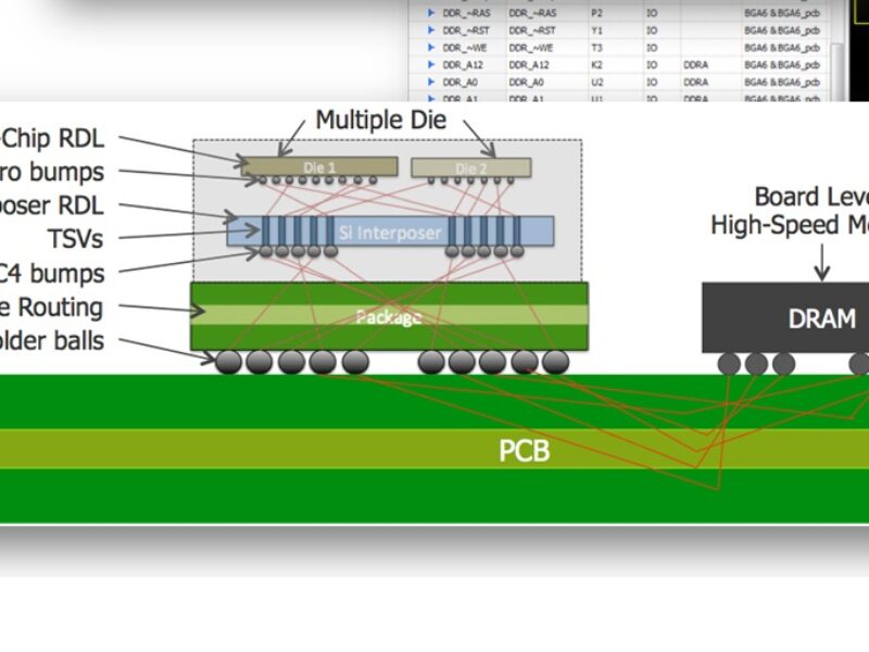
Mentor has addressed what it sees an issue of information exchange between design teams working at the interfaces between the physical aspects of integrated circuit/ASIC pinout; and the design and optimisation of custom IC packages; and the process of entering that package and pinout into the PCB place-and-route process. New packaging techniques – stacked dice, through-silicon vias and very hihg bump/pin counts – are forcing change, Mentor says.
There is necessarily a great deal of data that can be fed both forwards and backwards along that chain. An initial IC die-bump layout may call for a very complex pin assignment and interposer design within the IC’s package; looking a the constraints of the package design can generate feedback to the the IC pin placement that can subsequently simplify and cut costs in the package design. Similarly, an initial pin assignment on the package might demand a very complex routing escape pattern; a well-informed revision could simplify the board place-and-route, and save layers and costs. Where a change is necessary, it feeds back the required information to invoke a fresh run of an analysis tool, for example in areas such as signal integrity or thermal design

Mentor’s introduction addresses these “domain boundaries”. It does not link, in an active, “live windows” sense, the EDA packages used in each domain; but it facilitates extracting from each, just the data that is needed to pass key design information and constraints up and down the chain – automating a process that already takes place but with (sometimes cumbersome) manual and simple (e.g. spreadsheet) tools. It employs standardised data formats already established for exchange of data, and Mentor says it is vendor-agnostic in respect of any of the design tools used.
The Package Integrator solution automates planning, assembly and optimisation of complex multi-die packages. It incorporates a virtual die model concept for true IC-to-package co-optimisation. In support of early marketing-level studies for a proposed new device, users can plan, assemble and optimise complex systems with minimal source data. The Package Integrator flow allows design teams to realise faster and more efficient physical path finding and seamless tool integration for rapid prototyping, right to the production flow. In the term “path finding”, Mentor attempts to capture the process of finding and converging on the ideal, or at least an optimised, solution to a given layout task.
This solution ensures that ICs, packages and PCBs are optimised with each other to reduce package substrate and PCB costs by efficient layer reduction, optimised interconnect paths, and streamlined/automated control of the design process. The Xpedition Package Integrator product also provides the industry’s first formal flow for ball grid array (BGA) ball-map planning and optimisation based on an “intelligent pin” concept, defined by user rules. A multi-mode connectivity management system (incorporating hardware description language (HDL), spreadsheet and graphical schematic) provides cross-domain pin-mapping and system level cross-domain logical verification.
Features include:
• Cross-domain interconnect visualisation in a single view
• Powerful, comprehensive and user-friendly multi-mode physical layout tools with routing for PCB, MCM, SiP, RF, Hybrid and BGA designs.
• Fully automated library development
The Xpedition Package Integrator flow builds on other Mentor Graphics tools such as the HyperLynx signal and power integrity product, FloTHERM computational fluid dynamics (CFD) thermal modelling tools, and the Valor NPI substrate fabrication checking tool. To complete the Mentor Graphics co-design solution, Nimbic was acquired in 2014. The Nimbic technology provides Maxwell-accurate, 3D full-wave electromagnetic (EM) high-performance simulation solutions that accurately calculate complex electromagnetic fields for chip-package-board simulation.
Mentor Graphics; www.mentor.com/pcb/package-integrator
 If you enjoyed this article, you will like the following ones: don't miss them by subscribing to :