Stacked CMOS could overcome Forksheet limitations, says IMEC
Research institute IMEC has proposed how Complementary FETs (CFETs) with vertically stacked n- and p-type transistors could overcome limitations with Forksheet refinements to nanosheet FinFETs.
IMEC first discussed the Nanosheet, Forksheet and CFET up to four years ago (see Here comes the forksheet transistor, says IMEC) although it was not clear then which of these techniques might be adopted at which process nodes and by which semiconductor manufacturers.
The nanosheet is being introduced by Samsung and Intel in advanced nodes however the Forksheet transistor may present problems scaling with reduced numbers of tracks in standard cells. The issue is discussed in the paper ‘PPAC of sheet-based CFET configurations for 4 track design with 16nm metal pitch’ presented at the VLSI Technology Symposium.
Julien Ryckaert, IMEC’s vice president of logic in charge of compute scaling, commented on the institute’s website: “In a CFET architecture, n- and pMOS devices are stacked on top of each other. Stacking removes the n-p spacing from cell height considerations, allowing further maximization of the effective channel width, and, hence, the drive current. We can also use the resulting area gain to push track heights to 4T and below.”
There are a couple of ways of integrating the CFETs; called monolithic and the other is sequential processing in wafer-to-wafer bonding is used. One obvious method is to adapt the Soitec SmartCut method used to make fully-depleted silicon-on-insulator (FDSOI) wafers.
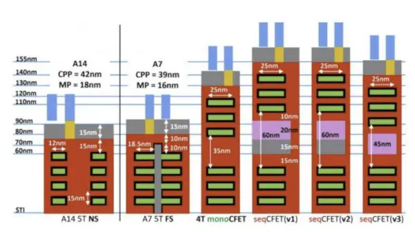
Gate cross sections for nansoheet (NS), forksheet (FS) and CFET (monolithic and sequential). Basic sequential CFET (=v1) is wider and taller than mono. With an optimized flow (including self-aligned gate merge (v2) and no gate cap (v3)), sequential CFET approaches monolithic CFET in terms of area consumption. Source: IMEC.
Ryckaert said: “From this benchmark, CFETs fabricated using a monolithic process flow are shown to consume less area and outperform their sequential counterparts, which suffer from a rise in effective capacitance. However, we show that we can put the trajectory of the sequential CFET on par with that of monolithic CFETs by applying three optimizations: (1) self-aligned gate merge, (2) omission of the gate cap and (3) the use of hybrid orientation technology, referred to as HOT.”
HOT refers to using different crystal orientations in the two wafers to favour the electron mobility in the nmos top layer and the hole mobility in the pmos bottom layer. The sequential method also raises concerns about thermal budget constraints for subsequent processing although these can be mitigated.
Ryckaert said that monolithic CFET is the preferred choice but the number of additional controls in sequential process control make it of interest.
The adaption of the SmartCut method is not only a possibility for sequential CFET process flows but could also provide more generic 3D sequential stacking for memory-on-logic and logic-on-logic. This could include the combination of traditional FinFET CMOS on one layer for performance with FDSOI CMOS on another.
Related links and articles:
News articles:
Here comes the forksheet transistor, says IMEC
Samsung to introduce nanosheet transistors in 3nm node
Intel renames manufacturing nodes, tips RibbonFET, PowerVia
IMEC proposes liquid memories for higher density storage
 If you enjoyed this article, you will like the following ones: don't miss them by subscribing to :