TI claims industry’s fastest 16bit DAC
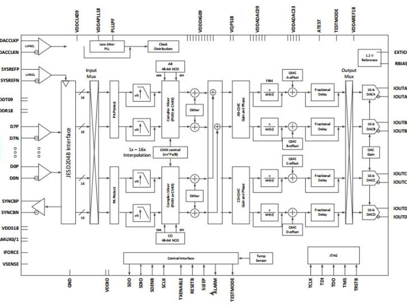
The 4-channel, 2.5-GSPS DAC38J84 is 66 percent faster than existing devices and supports the JEDEC JESD204B serial interface standard for data converters up to 12.5 Gbps. The pin-compatible 2-channel, 16-bit DAC38J82 also runs at 2.5 GSPS, 25 percent faster than existing 16-bit dual DACs.
The DAC38J84 and DAC38J82 provide the bandwidth, performance, small footprint and low power consumption needed for multi-mode 2G/3G/4G cellular base stations to migrate to more advanced technologies, such as LTE-Advanced and carrier aggregation on multiple antennas. The DACs support up to 2 GHz of information bandwidth for wideband power amplifier digital pre-distortion, millimeter wave backhaul infrastructure, signal jamming, radar and test equipment.
An interoperability report is available demonstrating the DAC38J84 with Altera’s Stratix V and Arria V FPGAs. The report provides the guidance designers need to quickly implement a working link between the FPGA and high-speed DAC.
The DACs provide an input rate up to 1.23 GSPS per DAC, with the DAC38J84 providing two independent transmit paths with up to 1 GHz of complex information bandwidth each – 67 percent more than the next fastest quad-channel DAC. This is also the first quad DAC to integrate a multi-band summation block that allows two complex carrier blocks to be independently mixed to the desired frequency before being summed together for a single path complex transmit. This supports up to 2 GHz of information bandwidth from one pair of 2.5-GSPS output DACs.
The DAC37J84 consumes only 1100 mW at the common wireless base station condition of 1.474 GSPS, 50 percent lower than existing 4-channel DACs. At 2.458 GSPS, the DAC38J84 uses only 1612 mW.
Evaluation modules (EVMs) are available to quickly evaluate the performance of the DACs. The DAC38J84EVM, DAC37J84EVM, DAC38J82EVM and DAC37J82EVM include the LMK04828, the industry’s first JESD204B clock jitter cleaner, which provides the 2.5-GHz DAC clock and multiple SYSREF signals for full JEDEC JESD204B multi-chip synchronization. An IBIS model is also available to verify board signal integrity requirements.
In Q2 2014, reference designs will be available for all four DACs. The designs will include the LMK04828 JESD204B clock jitter cleaner and two wideband complex modulator options for a complete bits-to-RF solution up to 4 GHz. Modulator options will include the TRF3705 and an upcoming version of the TRF3705 with integrated PLL/VCO.
Customers can pair any of the DAC EVMs above with the TSW14J56EVM pattern generator and data capture card, and a suitable analog-to-digital converter (ADC) EVM, such as the ADS42JB69EVM, to create a complete transmit and receive evaluation system.
Samples of all four DACs are available today in a 10-mm by 10-mm BGA package. Production quantities are expected in the first half of 2014. Suggested retail pricing for 1,000-unit quantities is as follows: US$120 for the DAC38J84, US$79 for the DAC37J84, US$70 for the DAC38J82 and US$39.95 for the DAC37J82.
www.ti.com/dac38j84-pr-eu
 If you enjoyed this article, you will like the following ones: don't miss them by subscribing to :