ZF and SiliconAuto introduce real-time I/O chip for autonomous driving
A new chip architecture aimed at simplifying high-performance computing for autonomous vehicles has been unveiled by ZF and SiliconAuto. The companies demonstrated a real-time I/O interface chip paired with a microcontroller at embedded world 2026 in Nuremberg, showing how sensor data for automated driving systems can be acquired and pre-processed directly in hardware.
The design targets next-generation Advanced Driver Assistance Systems (ADAS) and automated driving platforms, promising improved efficiency and flexibility compared with traditional monolithic SoC architectures. For engineers and system designers following automotive compute trends, the approach highlights a shift toward modular chiplet-based architectures and more open integration with AI inference engines.
Real-time sensor processing moves closer to the edge
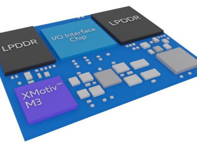
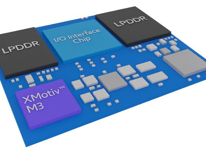
The joint demonstration centers on a newly designed ZF I/O interface chip that performs sensor data acquisition and pre-processing in real time. The device integrates multiple automotive sensor interface IP blocks and processing capabilities, including low-latency camera image signal processing and on-chip radar signal processing.
In the demonstration system, the chip works alongside SiliconAuto’s XMotiv M3 microcontroller, which acts as the system’s safety controller. Running at 160 MHz, the controller handles functions such as secure boot, power sequencing, clock management, and reset supervision.
One key design goal is reducing the burden on central compute processors. By handling sensor interfacing and early-stage processing locally, the interface chip limits data transfers to DDR memory and allows the main high-performance SoC to focus on perception and driving algorithms. According to the companies, this architecture can lower power consumption and improve overall system efficiency.
A modular alternative to monolithic automotive SoCs
The architecture also aims to give automotive OEMs greater freedom when choosing their compute platforms. Rather than relying on a single large SoC, the new design connects to a preferred performance processor using standardized high-speed interfaces such as PCIe or Ethernet.
This SoC-agnostic approach means that even processors without native automotive sensor interfaces — such as CSI-2, CAN, or LVDS — can be integrated into the system. As a result, carmakers can pair the interface chip with different AI inference engines or compute solutions depending on performance needs.
The platform is also designed to scale from entry-level ADAS applications to higher-end automated driving systems approaching SAE Level 4 autonomy. Modular chiplets allow individual components to be upgraded without redesigning the entire compute architecture.
Toward open automotive chiplet ecosystems
Looking ahead, the companies plan to support open die-to-die interconnect standards such as UCIe, enabling the I/O component to evolve into a fully compliant chiplet. This would allow OEMs to independently select compute, AI acceleration, and I/O components while maintaining long-term design flexibility.
The project also reflects broader European semiconductor goals. It was supported by Germany’s Federal Ministry for Education, Research and Space through the ZuSEKI-mobil program, which focuses on secure and sustainable microelectronics development in Europe.
Beyond flexibility, the companies argue that the modular chiplet strategy can extend the lifetime of high-performance automotive compute platforms while reducing energy consumption — an increasingly important factor as vehicles incorporate more sensors and AI processing capabilities.
 If you enjoyed this article, you will like the following ones: don't miss them by subscribing to :