Breaking free of epitaxial constraints
Researchers at USC in California have removed the traditional epitaxial constraints challenging the direct growth of a vast array of crystalline compound semiconductors on amorphous and non-epitaxial substrates.
This means they could potentially grow highly heterogeneous electronic and photonic devices directly on silicon and other substrates such as glass and plastics without ever relying on costly epitaxial transfer techniques.
Using a thermodynamic model of confined liquid metal wetting, the researchers first derived a wetting phase diagram for templated liquid metals, showing there are multiple classes of templating behaviour for a number of relevant materials, with a geometrically driven wetting condition for the templated liquid metals for any substrate surface energy.
They then demonstrated that InP, GaP, InAs, InGaP, SnP, and Sn4P3 crystals can be grown directly on SiO2, Si3N4, TiO2, Al2O3, Gd2O3, SrTiO3, and graphene, making their approach truly general.
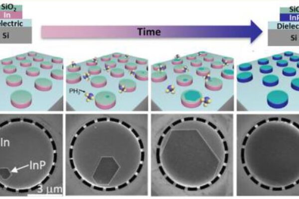
As a practical demonstration, the authors grew InP in an indium template using the TLP technique. They first deposited Indium metal with standard evaporation of sputtering techniques on a Gd2O3 substrate, with a capping silicon oxide layer. They then patterned and heated the substrate under hydrogen so the metal would melt, yet retain its original deposited geometry (the template that is, without de-wetting from the substrate).
Introducing a precursor gas at the growth temperature causes supersaturation and a precipitation of the target material directly into the melted metal, with the latter being consumed as the nucleus grows, the paper reports. The end result is a single crystal with the exact geometry of the initial melted metal template (they had worked with circular templates about 5µm in diameter). The authors also grew phase pure templated crystalline Sn4P3 on a silicon/SiO2 substrate.

Pushing their TLP technique demonstration one notch further, they even grew dual compound mesas with an atomically sharp lateral heterojunction between indium phosphide and tin phosphide, despite the two materials having vastly different crystal structures.
The seemingly simple trick explained in the paper was to heat an array of neighbouring indium and tin mesas to 550°C before introducing precursor gas phosphine. At that temperature, the two metals mixed completely in their liquid phase, and the introduction of a controlled phosphine (PH3) flux triggered the simultaneous, yet separate growth of single indium phosphide and tin phosphide crystals from the unique In/Sn melt.
Because it allows the growth and manufacture of crystalline materials without requiring a nearly lattice-matched substrate, the TLP growth process for which the researchers have filed a provisional patent could enable the design of entirely new crystalline materials (for which traditional vapour-phase epitaxy lacked a suitably matching substrate). This could lead to many new electronic and photonic devices difficult or near impossible to create so far.
The authors conclude that such a TLP growth process will enable device integration at the microscale, way beyond today’s coarse 3D integration (physical stacking).
pubs.acs.org/doi/abs/10.1021/acsnano.8b01819
 If you enjoyed this article, you will like the following ones: don't miss them by subscribing to :