Building flexible microprocessors from 2D-material transistors
The device can execute user-defined programs stored in an external memory, perform logical operations and communicate with its periphery. What’s more, the design is readily scalable to multi-bit data, the researchers claim, hoping these ultra-thin devices, flexible
Their paper “A microprocessor based on a two-dimensional semiconductor” published in Nature Communications explains that although the microprocessor was fabricated in gate-first technology on a silicon wafer with 280-nm-thick silicon dioxide, the silicon wafer was merely used as a carrier medium and could easily be replaced by glass or any other material, including flexible substrates.
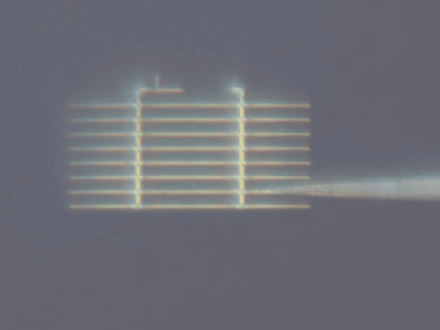
“We fabricated 18 devices per wafer, with FET channels made from chemical vapour deposition (CVD) grown large-area bilayer MoS2 films. Two Ti/Au metal layers were used to interconnect the transistors and Al2O3 was used as gate oxide”, the researchers write in their paper. The MoS2 FET devices exhibited a field-effect mobility of around 3cm2 V−1 s−1, a threshold voltage VT of about 0.65V, an on/off ratio of about 108, and uniform behaviour over a 50mm2 area over the wafer.

Minimum feature size was kept to 2μm to make the design immune to sample in-homogeneities (such as small holes, cracks and contaminations in the MoS2 film) and also allows for fast visual inspection of the lithographic structures with an optical microscope. The circuit is based on the NMOS logic family, where both pull-up (load) and pull-down networks were realized using n-type enhancement-mode FETs with Width/Length ratios of 45/2 (μm/μm) and 7/5, respectively.
Transistor count was minimized for demonstration purposes, hence the single-bit data handling capability of the proof-of-concept 2D microprocessor. “We stress that this is not a fundamental limitation and the device is readily scalable to N-bit data, broadly speaking by connecting N of our devices in parallel“, the researchers wrote.
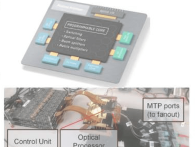
The bare bone device comprises all the basic building blocks common to most microprocessors, including an arithmetic logic unit (ALU), which for simplicity was implemented to only perform logical conjunction and disjunction operations, an accumulator (AC), which holds one of the operands to be supplied to the ALU, an instruction register (IR) that stores the content of the program memory currently being executed, a control unit (CU) that receives as input the instruction code from the IR and orchestrates all resources by enabling components to access the internal bus via the control signals EA and EO; a program counter (PC) which supplies the memory with the address of the active instruction and an output register (OR) that allows the processor to transfer the results of a calculation to the output port. Memory was implemented off-chip.

Subunits, such as for example, the ALU or the IR, were provided with metal pads for individual testing in a wafer probe station.
Because no metal catalyst was required for the synthesis of the MoS2 films, the researchers are confident they could growth such devices directly on flexible substrates. Because the 2D semiconductor materials are so thin, only a few atoms thick, and thanks to their excellent electrical properties, they are inherently flexible and compact which make them suitable for fully flexible electronic devices.

Credit: Hermann Detz, TU Vienna
Lead researcher on this project, Thomas Mueller from TU Vienna expects such processor circuits to be combined with light emitters (also made with MoS2) to make flexible displays and e-paper, or sees them integrated as logic circuits in smart flexible sensors. Next on the researchers’ roadmap is a full 8-bit design, with smaller feature sizes.
“Our approach is to improve the processing to a point where we can reliably make chips with a few tens of thousands of transistors” commented Dmitry Polyushkin (TU Vienna), an author of the work on the Graphene Flagship project page.
Graphene Flagship – https://graphene-flagship.eu
Related articles:
European graphene initiative doubles its size with new funding
Graphene enables electrical control light emitter energy flows
Imec aims 8-bit plastic MPU at smart labels
Roll-to-roll flexible electronics to hit 100GHz?
Starting all over again on plastic: ARM
 If you enjoyed this article, you will like the following ones: don't miss them by subscribing to :