First Bizen quantum tunnelling transistors launched
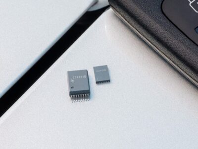
The first devices to use the Bizen process technology include three parts rated at 1200V/75A, 900V/75A and 650V/32A, available in the industry-standard TO247 or TO263 power MOSFET packages. These are made using standard silicon substrates on conventional, larger-geometry silicon processing lines. The initial pilot line for testing the Bizen technology was set up at Semefab in Scotland.
“To get this level of performance from traditional silicon-based MOSFETs, the device size must be much bigger. 1200V/75A in a TO247 housing can be achieved using wide bandgap materials like silicon carbide, but this approach has other well-known issues,” said David Summerland, CEO and founder of Nottingham-based Search For The Next (SFN) which developed the Bizen technology. This is being used for the parts, called Quantum Junction Transistors (QJT), from subsidiary Wafertrain.
“SiC, for example, takes much longer to process and has a significant manufacturing carbon footprint. Also, regardless of the roadmaps, SiC does not scale like silicon, and the economic argument that SiC can match silicon does not take into account the advances made possible by Bizen. By contrast, the data we have obtained from physical wafer tests proves that by using Bizen on silicon substrates, our QJTs deliver the same performance as SiC or GaN. Yet the production equipment required to make a QJT is exactly the same as for a standard silicon MOSFET, and the Bizen process adds no extra manufacturing complexity.”
Bizen applies quantum tunelling to a traditional bipolar wafer process. The result is a very rugged and reliable device with the heritage and pedigree of traditional bipolar silicon technology. Bizen also reduces leadtimes from 15 weeks for a CMOS device (although not a SiC MOSFET) to less than two weeks, and halves the number of process layers. The QJTs use these same eight layer bipolar process.
Wafer tests also show that the Bizen process exhibits an effective current gain of over 1 million, says Summerland. This will enable direct connection between the 1200V/75A QJT power transistor and a low voltage, low current CPU output port such as a PWM for a monolithic design.
“The QJT is the first power device on the Bizen family roadmap. This will shortly lead to the PJT (Processor Junction Transistor), an integrated Bizen device with its own processor which can also be produced on a manufacturing cycle time of eight days, heralding a new era of intelligent power devices,” he said.
SFN has also released other comparative performance metrics for a 1200V/100A part – also in TO247 – which is on its short-term roadmap. The losses at rated current will be a quarter (<300mV) of those exhibited by the SiC device, and its input capacitance will also be four to five times less (< 1pF).
In July Semefab also started making 1200V Schottky diodes on an SiC process and is planning 1700V devices.
Related articles
Other articles on eeNews Europe
- Automotive software house Aurora Labs receives $23 million in funding
- ARM Nvidia deal is wakeup call to industry
- IBM aims for million qubit quantum computer
- SiFive takes on ARM with CEO from Qualcomm
- Ericsson in $1.1bn IoT buy
 If you enjoyed this article, you will like the following ones: don't miss them by subscribing to :