Grown on silicon: blue–violet InGaN laser diode operates at room-temperature
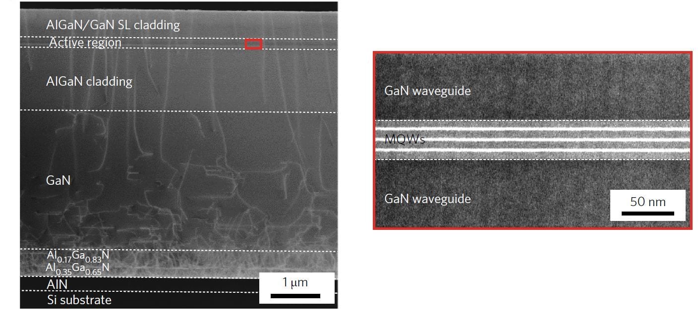
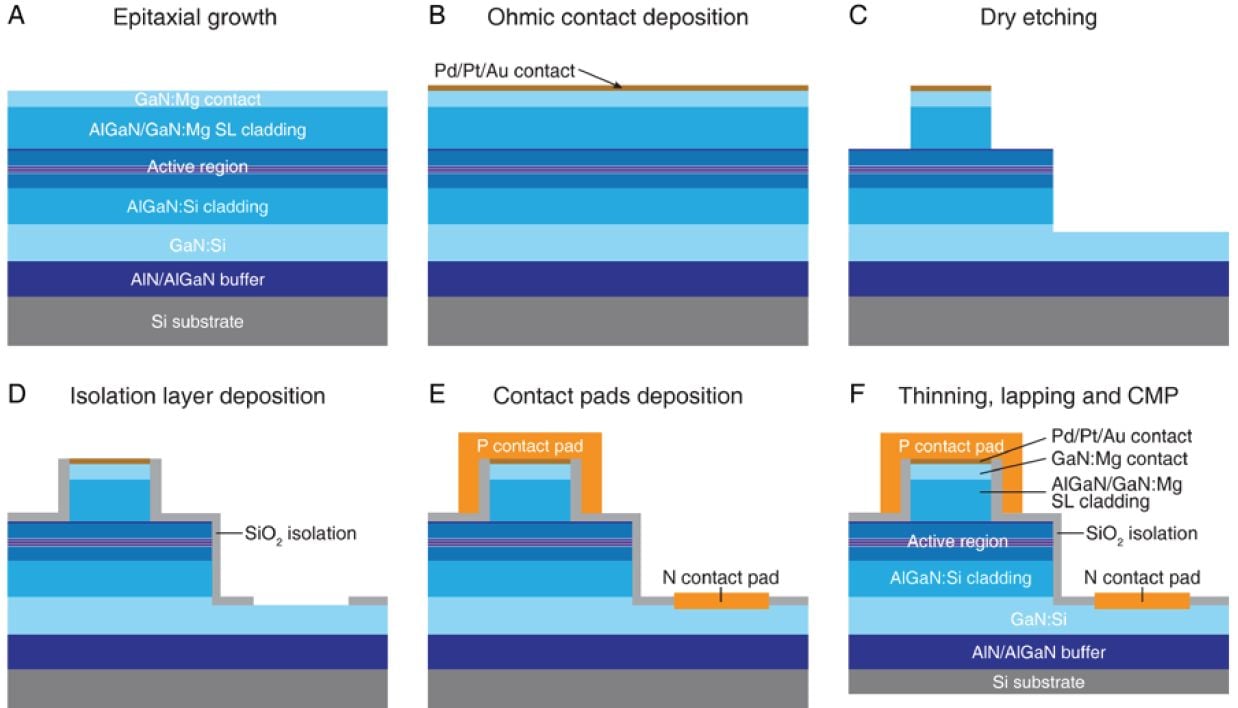
In a paper recently published in Nature Photonics Letters titled “Room-temperature continuous-wave electrically injected InGaN-based laser directly grown on Si”, they describe how a carefully engineered Al-composition step-graded AlN/AlGaN multilayer buffer between the Si and GaN successfully eliminated crack formation while also reducing the dislocation density.
Often, one way to circumvent the large lattice mismatch between GaN and Si (around 17%) is to integrate GaN laser diodes on silicon through heterogeneous chip-bonding, or designing the whole laser and driving circuitry on costly GaN wafers for later SiP integration. On monolithically integrated devices, because GaN shrinks twice as fast as Si when cooling down from the high process temperatures necessary for epitaxial growth (due to the difference in their CTE), defects and networks of micro-cracks propagate through the device, drastically lowering operation efficiency and yield.
Here, the multilayer stack was build up so as to effectively manage mismatch-induced lattice stress. By inserting the carefully designed Al-composition step-graded AlN/AlGaN multilayer buffer, the scientists were able to build up enough compressive strain to not only compensate for the tensile stress due to the CTE mismatch during cool down, but also to induce the inclination and annihilation of threading dislocations (TDs) at the interfaces.
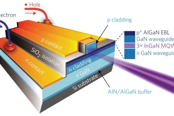
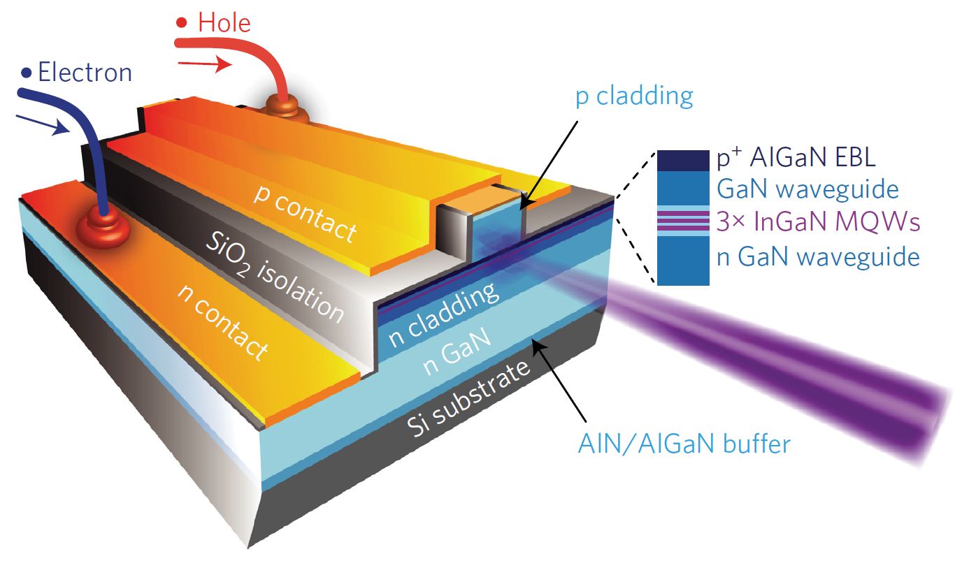
What they designed in the end, was a blue–violet Multi-quantum wells InGaN laser diode sandwiched between two GaN layers acting as the waveguide, the whole device being directly grown on silicon throughMetal-Organic Chemical Vapour Deposition (MOCVD). The as-grown GaN-on-Si laser diode epitaxial wafer was processed into ridge-shaped devices measuring 4×800μm2.
diode directly grown on Si.
Emitting at the 413nm wavelength under continuous-wave current injection at room temperature, the whole device build up is around 6 μm thick (for an active layer just under 50nm thick). This includes both the upper and lower optical cladding layers. The device lased with a threshold current density of 4.7 kA cm–2.
The researchers also reported a very small wafer bow (under 10μm), which means the devices could be produced reliably in volume with a high yield.
Another process simplification is that because the waveguide and cladding layers confine most of the stimulated emission photons in the active region, the stimulated photons are not absorbed by the underlying Si, making its removal unnecessary.
Operational lifetime was limited though, due to excessive heating. But the researchers hope to improve the device’s lifetime by further reducing the TD density in the GaN film through epitaxial lateral overgrowth on Si and by optimizing the growth conditions of the active region. They see this novel GaN-on-Si laser construction as a potential on-chip light source for future monolithic-integrated Si photonics.
The corresponding author of the paper, Professor Qian Sun from SINANO, CAS told eeNews Europe that he does plan to commercialize GaN-on-Si laser diodes and has patented a few key technology pieces relating to their fabrication. He is also interested in collaboration with industrial partners to speed up their commercialization.
Related articles:
Quantum dots shrink on-chip lasers to 1μm
Vertical nanolasers open optical ports out of silicon
Nanolaser enables on-chip photonics
 If you enjoyed this article, you will like the following ones: don't miss them by subscribing to :