Grown on silicon: QD-based micro-ring GaAs lasers operate from 0.6mA
Emitting at 1.3μm, the micro laser was tested under continuous-wave lasing at up to 100°C, making it very promising for integration into compact optical communication systems.
Their paper “1.3 μm submilliamp threshold quantum dot micro-lasers on Si” published in the Optica journal reveals a novel GaAs-on-Si heterogeneous growth strategy which confines dislocations and growth defects and allows for direct growth on silicon with no germanium buffer layer or substrate miscut. This was combined with a quantum dot (QD)-based active medium, known to effectively alleviate the negative influence of dislocations and surface recombination arising from lattice-mismatched growth and device fabrication.

First, the researchers etched V-grooves along the [100] direction on a (001) silicon substrate, which they filled with an array of GaAs in-plane nanowires grown directly inside the silicon V-grooves by selective-area metal-organic chemical vapor deposition.
Then further GaAs was grown including 15 periods of Al0.3Ga0.7As∕GaAs (5/5nm) superlattice for annihilating the threading dislocations. Eventually the GaAs nanowires were coalesced into a 1.5μm-thick continuous and smooth surface, on top of which a GaAs∕AlxGa1−xAs graded-index separate-confinement laser heterostructure was grown in a molecular beam epitaxy system. This included seven InAs/InGaAs quantum dot-in-a-well layers incorporated in the laser active region, with a quantum dot density approaching 6×1010 cm−2.
The paper reports that the 4.1% lattice mismatch between GaAs and silicon was mostly accommodated by the formation of a few nanometer-thick stacking faults in the V -grooved structure, enabling the fabrication of a defect-free GaAs laser with performances comparable to devices built on a native GaAs substrate.
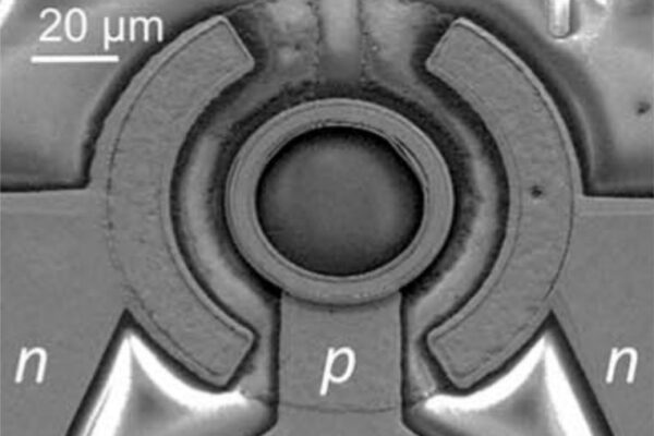
Out of that stack, the researchers patterned the ring structures of various whispering gallery mode (WGM) lasers with radii ranging from 5 to 50μm and ring widths ranging from 2 to 7μm wide. The paper notes that a 4μm-tall mesa allowed a strong lateral optical confinement supporting excellent cavity modes and enabling very low-threshold lasing. The scaled-down 10μm wide device (with a 5μm radius) gave the lowest lasing threshold, down to 0.6mA.

The researchers see their direct III–V/Si epitaxy fabrication method as a promising alternative to wafer-bonding techniques currently used to integrate light sources on silicon. This could pave the way to denser photonic integration while maintaining low power operation.
On their roadmap, the authors plan to integrate in-plane coupling waveguides for the efficient extraction/coupling of the lasing light while trying to further improve the overall performance of their devices beyond that of heterogeneously bonded light sources. The researchers have secured several patents and make their technology available for licensing.
Related articles:
Nanowire array lasers readily coupled to waveguides
Grown on silicon: blue–violet InGaN laser diode operates at room-temperature
CMOS electronics and silicon photonics integration aims at 1Tb/s
 If you enjoyed this article, you will like the following ones: don't miss them by subscribing to :