How about plastic MEMS?
The work on plastic MEMS is largely inspired from the micro-cantilever silicon MEMS used as electronic-noses, with adequate surface functionalization on the cantilever beam so that target molecules can be adsorbed to the surface of the cantilever and modify its flexure (in a static mode, through added mass) or its resonant frequency (in a dynamic sensing mode).
As it is the case for many printed electronic applications using polymers, Ayela summarized the benefits: a combination of low-cost synthesis, the good processability of organic materials and a large spectrum of optical, mechanical, electrical and chemical properties that can be accurately tuned to attain a specific functionality. But a key motivation behind the use of polymers in MEMS devices is the materials’ low values of Young’s modulus, making the devices extremely flexible, ensuring large deflections even under a low stimulus, Ayela highlighted.
In fact, although today’s commercial MEMS applications solely rely on silicon or glass-based devices, abundant literature revolves around polymer MEMS sensors and actuators built on substrates as diverse as Polystyrene, Polypropylene, Polyimide, cyclic olefin copolymer resins or the SU-8 epoxy-based photoresist to name a few.

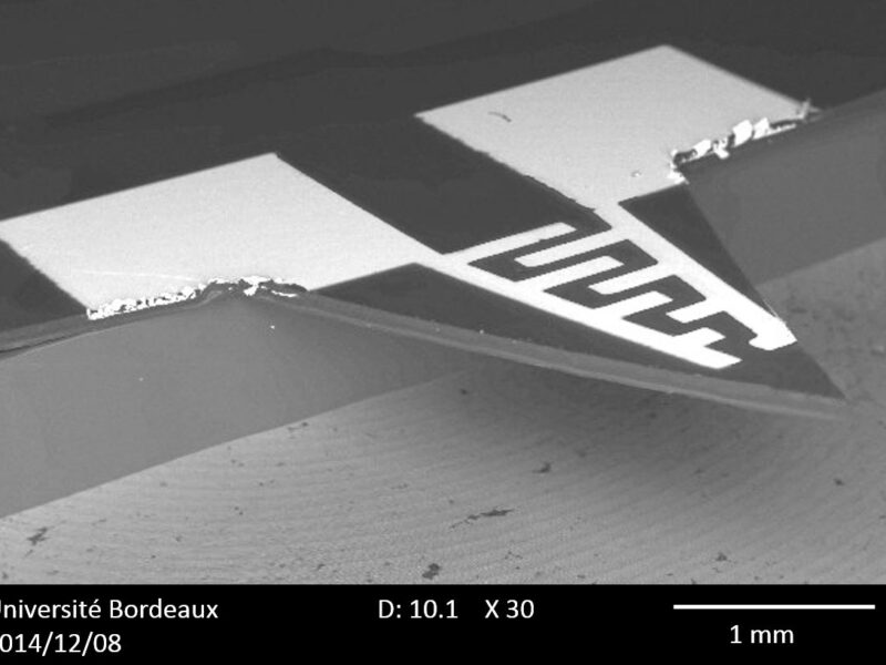
Here, Ayela leveraged the well-known piezoelectric properties of copolymer poly[(vinylidenefluoride-co-trifluoroethylene, abbreviated P(VDF-TrFE) to design a piezoelectric OFET (Organic Field Effect Transistor) integrated into a micro-cantilever made of flexible Polyethylene Naphthalate (PEN). His results published in Nature’s Scientific Reports under the title “Piezoelectric polymer gated OFET: Cutting-edge electro-mechanical transducer for organic MEMS-based sensors” revealed that extremely sensitive MEMS sensors could be made, detecting strains from very low beam deflections.
Designed to operate as a mechano-electrical transducer, the triangular-shaped piezoelectric OFET stacks a bottom aluminium gate electrode, P(VDF-TrFE) and poly(1-vinyl-1,2,4-triazole) (PVT) gate dielectric layers, an organic semiconductor (Pentacene gave the best results) and gold source-drain (S/D) electrodes at the top. First, a polarization step is required to induce piezoelectricity (creating polarization states in the material), this was done with successive high-voltage sweeps across the gate and the source. But then as the cantilever is deflected (by added molecular mass from a target molecule), the mechanical strain changes the distance between hydrogen and fluorine atoms in the P(VDF-TrFE) layer, leading to a depletion of positive charge in the p-type semiconductor. This directly affects the OFET’s characteristics, hence realizing a highly sensitive mechano-electrical transducer.
To fabricate the OFET-embedded MEMS, Ayela and his team combined classical deposition techniques (using shadow masks) with xurography, a sort of high-precision cutting plotter offering a lateral resolution of 5µm. The simple fabrication process eliminates the need for the complicated etching steps and lithographic masking required in silicon processing, making such MEMS very cost competitive, while the yield of operating devices is quite high at 95%.
In one implementation, the OFET-embedded sensor had been functionalized with a hydrogel layer on top. Compatible with printing technologies, the hydrogel swells in the presence of humidity, creating a tensile strain and flexing the cantilever as relative humidity increases. In their paper, the researchers reported a record linear relative strain sensitivity of 600 at low strain level (below 0.3%), with a measured sensitivity of 7500ppm/%RH and an extracted limit of detection of 0.2%RH. Ayela anticipates that with such a high sensitivity to strain, many more OFET-embedded MEMS sensor could be designed, to be mass-produced at low cost.
Asked if such MEMS, lacking the hard shell packaging of conventional silicon MEMS would be fragile, the researcher claims on the contrary that because they are so flexible, his plastic MEMS are much more rugged and return to their original state after an impact, they still need to have some form of encapsulation, with an undercut area but this could be done within a laminated process.
In fact, Ayela told eeNews Europe that such OFET-embedded MEMS can easily be manufactured using industrial processes, including roll-to-roll fabrication techniques. According to him, such devices are commercially viable for integration in smart packages. On an academic level, the cheap OFET-embedded cantilevers could also be used to accurately characterize the electromechanical response of organic semiconductors, something the researchers are already doing: they have recently published a paper titled “Unusual electromechanical response in rubrene single crystals” using the OFET-embedded MEMS as a test platform while trying to improve its electromechanical sensitivity with more sensitive organic semiconductors.
Organic Electronics & Microsystems Group IMS Laboratory Université de Bordeaux – oembordeaux.cnrs.fr
Related articles:
Starting all over again on plastic: Arm
Flexible electronics scale up to billions with fab-in-a-box
Piezo-mems vibration energy harvesters enable smartmesh IP wireless sensor network
UCB reports printed MEMS switches
 If you enjoyed this article, you will like the following ones: don't miss them by subscribing to :