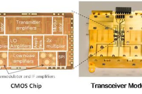
Millimeter-band CMOS chip communicates at 56Gbps
Millimeter-waveband (30-300 GHz) could bring high-capacity wireless communications in places where fibre-optic networks would be difficult to lay. But designing CMOS integrated circuits running at such high frequencies remain a challenge. The two labs were able to design low-loss transceiver circuits that modulate and demodulate broadband signals into and out of the millimeter-waveband, connecting the circuit board to the antenna.

Fig.1: Transceiver CMOS chip (left) and module (right).
First, Tokyo Institute of Technology developed a technology for broadband, low-loss transceiver circuits in which data signals are split in two, with each converted to different frequency ranges, and then recombined – see figure 2.

Fig.2: Transceiver configuration.
Each signal is modulated into a band 10-GHz wide, with the low-band occupying the 72-82 GHz range, and the high-band occupying the 89-99 GHz range. This technology enables modulation on an ultra-wideband signal of 20 GHz, with low noise and a similar range in the ratio between input and output power as existing 10 GHz band methods, which results in high-quality signal transmissions.
The research institute also developed an amplifier to send and receive radio waves signals converted to the millimeter-waveband. The ultra-wideband amplifier for 72 to 100 GHz was designed with circuit technologies that stabilize the amplification ratio by feeding the amplitude of the output signal back to the input side for signal components whose amplification ratio decreases based on frequency.
The signal converted to the millimeter-waveband by the semiconductor chip is transported over the circuit board’s signal path and supplied to the antenna. Because the antenna is made out of a waveguide (a metallic cylinder), there needs to be an ultra-wideband, low-loss connection between the printed circuit board and the waveguide.
Fujitsu Laboratories and Tokyo Institute of Technology developed an interface between the circuit board and waveguide that uses a specially designed pattern of interconnects on the printed circuit board to adjust the impedance for the ultra-wideband range, enabling loss in the desired frequency range to be greatly reduced.
In this development project, Tokyo Institute of Technology was primarily responsible for reducing transceiver-circuit losses and developing broadband technologies, while Fujitsu Laboratories mainly handled modularization technologies.
Performing indoor data-transfer tests with two modules facing each other separated by a distance of 10cm, the Japanese researchers achieved data-transfer rates of 56 Gbps, the fastest wireless transmission speeds in the world, with a maximum loss of 10% between the waveguide and circuit board. Fujitsu Laboratories aims to have a commercial implementation of wireless trunk lines for cellular base stations around 2020.
Visit the Tokyo Institute of Technology at https://www.titech.ac.jp/english/
Visit Fujitsu Laboratories at https://jp.fujitsu.com/labs/en
 If you enjoyed this article, you will like the following ones: don't miss them by subscribing to :