Room-temperature interface improves gallium nitride cooling
The surface-activated bonding technique developed at Georgia Tech in the US with researchers from Meisei University and Waseda University in Japan uses an ion source in a high vacuum environment to first clean the surfaces of the gallim nitride and diamond.
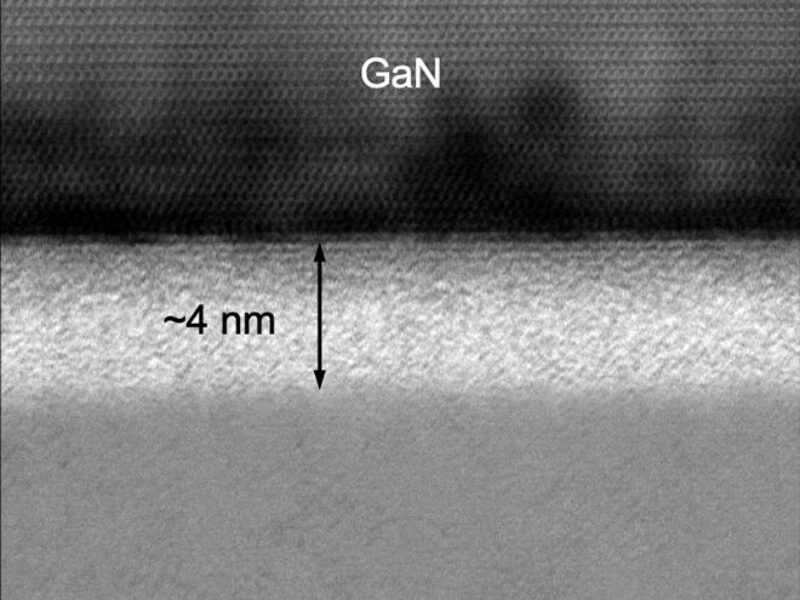
Activating the surfaces by creating dangling bonds and introducing small amounts of silicon into the ion beams facilitates forming strong atomic bonds at room temperature, allowing the direct bonding of the GaN and single-crystal diamond via a 4nm layer.
This allows heat dissipation up to twice as efficient as current GaN-on-diamond transistors to allow higher power levels, longer device lifetime, improved reliability and reduced manufacturing costs. Operating at room temperature also reduces the thermal stress applied to the devices.
“This technique allows us to place high thermal conductivity materials much closer to the active device regions in gallium nitride,” said Prof Samuel Graham at Georgia Tech’s George W. Woodruff School of Mechanical Engineering. “The performance allows us to maximize the performance for gallium nitride on diamond systems. This will allow engineers to custom design future semiconductors for better multifunctional operation.”
Heat dissipation can be a limiting factor in high power designs. Adding a layer of diamond, which conducts heat five times better than copper, allows engineers to spread and dissipate the thermal energy.
“In the currently used growth technique, you don’t really reach the high thermal conductivity properties of the microcrystalline diamond layer until you are a few microns away from the interface,” said Graham. “The materials near the interface just don’t have good thermal properties. This bonding technique allows us to start with ultra-high thermal conductivity diamond right at the interface.”
By creating a thinner interface, the surface-activated bonding technique moves the thermal dissipation closer to the GaN heat source.
“Our bonding technique brings high thermal conductivity single crystal diamond closer to the hot spots in the GaN devices, which has the potential to reshape the way these devices are cooled,” said researcher Zhe Cheng at Georgia Tech. “And because the bonding takes place near room temperature, we can avoid thermal stresses that can damage the devices.”
That reduction in thermal stress can be significant, going from as much as 900 megapascals (MPa) to less than 100 MPa with the room temperature technique. “This low stress bonding allows for thick layers of diamond to be integrated with the GaN and provides a method for diamond integration with other semiconductor materials,” said Graham.
Next: Bonding gallium oxide and silicon carbide
Beyond the GaN and diamond, the technique can be used with other semiconductors, such as gallium oxide, and other thermal conductors, such as silicon carbide. Graham said the technique has broad applications to bond electronic materials where thin interfacial layers are advantageous.
“This new pathway gives us the ability to mix and match materials,” he said. “This can provide us with great electrical properties, but the clear advantage is a vastly superior thermal interface. We believe this will prove to be the best technology available so far for integrating wide bandgap materials with thermally-conducting substrates.”
“We have the ability to choose processing conditions as well as the substrate and semiconductor material to engineer heterogenous substrates for wide bandgap devices,” said Graham. “That allows us to choose the materials and integrate them to maximize electrical, thermal and mechanical properties.”
 If you enjoyed this article, you will like the following ones: don't miss them by subscribing to :