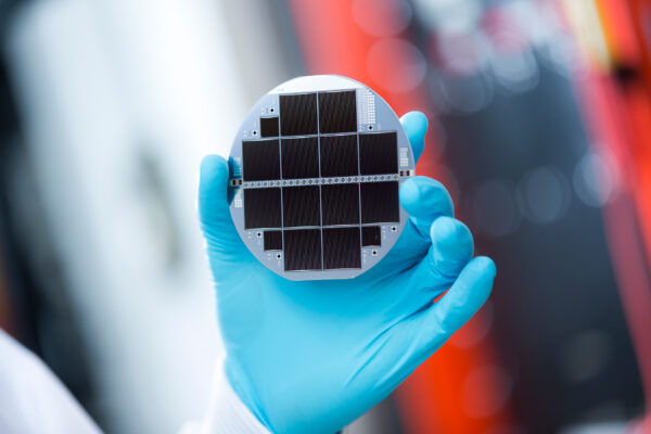
Silicon-based dual junction solar cell reaches 33.3% efficiency
Publishing their results in Nature Energy under the title “III–V-on-silicon solar cells reaching 33% photoconversion efficiency in two-terminal configuration”, the researchers report they demonstrated a III–V/Si cell reaching similar performances to standard III–V/Ge triple-junction solar cells.
Back in November 2016, the solar researchers in Freiburg together with their industry partner EVG had demonstrated an efficiency of 30.2 percent, increasing it to 31.3 percent in March 2017. Now they have succeeded once again in greatly improving the light absorption and the charge separation in silicon, thus achieving a new record of 33.3 percent efficiency.
The “direct wafer bonding” process used to transfer III-V semiconductor layers only 1.9 micrometres thick to silicon was performed with EVG’s EVG580 ComBond chamber after the surfaces had been deoxidized under high vacuum with an ion beam. Then in a pressurized environment, the atoms on the surface of the III-V subcell form bonds with the silicon atoms, creating a monolithic device. The researchers addressed key issues of multi-junction cells such as III–V/Si interface recombination and silicon’s weak absorption by using poly-silicon/SiOx passivating contacts and a novel rear-side diffraction grating for the silicon bottom cell.
The III-V / Si multi-junction solar cell consists of a sequence of subcells stacked on top of each other. So-called “tunnel diodes” internally connect the three subcells made of gallium-indium-phosphide (GaInP), gallium-arsenide (GaAs) and silicon (Si), which span the absorption range of the sun’s spectrum. The GaInP top cell absorbs radiation between 300 and 670 nm. The middle GaAs subcell absorbs radiation between 500 and 890 nm and the bottom Si subcell between 650 and 1180 nm, respectively. The III-V layers are first epitaxially deposited on a GaAs substrate and then bonded to a silicon solar cell structure. Here a tunnel oxide passivated contact (TOPCon) is applied to the front and back surfaces of the silicon. Subsequently the GaAs substrate is removed, a nanostructured backside contact is implemented to prolong the path length of light. A front side contact grid and antireflection coating are also applied.
 On the way to the industrial manufacturing of III-V / Si multi-junction solar cells, the costs of the III-V epitaxy and the connecting technology with silicon must be reduced. There are still great challenges to overcome in this area, which the Fraunhofer ISE researchers intend to solve through future investigations. Fraunhofer ISE’s new Center for High Efficiency Solar Cells, presently being constructed in Freiburg, will provide them with the perfect setting for developing next-generation III-V and silicon solar cell technologies. The ultimate objective is to make high efficiency solar PV modules with efficiencies of over 30 percent possible in the future.
Fraunhofer ISE – www.ise.fraunhofer.de
Related articles
Energy democratization will come: it’s called multi-junction photovoltaics
Researchers exceed theoretical efficiency limit for Si solar cells
Swiss consortium to set up pilot line for heterojunction solar cells
French-German collaborators claim solar cell efficiency world record
Tandem photovoltaics for record efficiencies?
 If you enjoyed this article, you will like the following ones: don't miss them by subscribing to :