Tactile skin gives prosthetics and robots a flexible touch
Dr Ravinder S. Dahiya, who joined the University of Glasgow last year as a senior lecturer in electronic and nanoscale engineering, will be leading the four-year research programme.
“To date, no robotics scientist has been able to create ultra-flexible tactile skin. Either the sensors have been too big or the electronics not sufficiently flexible”, explains Dr Dahiya who wants to get away from discrete and bulky silicon devices.
“Often, you see discrete components soldered on flexible PCBs, or hard component islands grafted onto flexible substrates. Some sensors may be flexible, but you need to connect them to electronic processing modules away from the sensing area, hidden in the robot’s housing” says Dr Dahiya whose vision is to integrate ultra-thin and flexible silicon-based electronics onto flexible polymers, in effect, forming sheets of distributed electronics along the sensors.
Printed organic electronics is typically seen as a good candidate for low-cost flexible sensing applications, but they have low charge carrier mobility, typically three orders of magnitude lower than that of single crystal silicon. Their short lifetime also makes organic electronics more suitable to low-cost disposable applications. These are real drawbacks if one is to rely on fast transistor switching speed for efficient data processing or communication needs, hence the researcher’s focus on using ultra-thin silicon-based devices.
In previous research, Dr Dahiya has developed tactile sensing chips, forming 5×5 arrays of Piezoelectric Oxide Semiconductor Field Effect Transistor (POSFET) pressure and temperature sensors, about 15x15mm in size.

Fig. 1: In the top close-up photo, serpentine shaped metal lines make up a passive device on two 15×22mm flex–chips, shown placed on 18mm and 30mm diameter cylinders.
Measuring 1x1mm, each POSFET tactile pixel in the arrays were obtained by spin coating piezoelectric polymer films directly onto the gate area of Metal Oxide Semiconductor (MOS) transistors. They were designed to yield human like spatial acuity, each tactile pixel being about 1mm apart.
After proving the sensor concept, Dr Dahiya looked into the formation of ultra-thin flexible silicon circuits. In a 2013 paper titled “Bendable Ultra-Thin Chips on Flexible Foils”, he demonstrated a top-down approach to design 1D (nanowires) and 2D silicon structures to be transferred as ultra-thin circuits onto thin flexible polyimide foils.
The so-called flex–chips were designed using regular semiconductor lithography and etching, but then various wafer thinning and structure dig-out tricks were performed in order to peel-off the 15μm thin devices from their original substrate onto a PDMS (Polydimethylsiloxane) film as a carrier before a final print-transfer onto a polyimide foil.
This transfer method was successfully applied to ultra–thin flex–chips from 4.5 to 15mm wide and from 8 to 36mm long, mostly featuring passive structures such as metal interconnects. The bending radius achievable without breaking was around 0.5mm, much smaller than what would be typically needed, told us Dr Dahiya.
Of course, this top-down approach gives a lot of control over the Si microstructures, their geometry, their crystallinity and doping levels. But in his newly funded research, Dr Dahiya aims for a much lower cost design methodology.
Following a bottom-up approach, he aims to grow vertical silicon nanowires on a gold catalyst, then harvest them and use them in a roll-to-roll dry printing process, very much like a toner of nanowires applied on a “pre-patterned” polymer foil.
The key challenge in this bottom-up approach is to be able to precisely align the harvested nanowires onto very well defined patterns to design the final circuits, but Dr Dahiya says he has several self-aligning tricks in mind to make this work as printable networks of distributed sensors.
Some of these tricks could include a form of optical or heat exposure of the polymer films to prepare them to receive the nanowire toner, some form of lithographic steps at the device and circuit level maybe, but Dr Dahiya was reluctant to say too much as he is in the process of patenting this new approach.
He will be working in collaboration with Professor Duncan Gregory, Chair in Inorganic Materials in the School of Chemistry, on the creation of the silicon nanowires. By developing a printing technique for high-mobility materials such as silicon, he hopes to combine the high-performance of Si electronics at a low cost base. In principle, other types of nanowires could be developed and used for printing electronic circuits, and nanocarbon tubes could also be on the agenda.

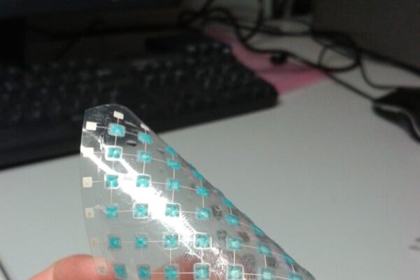
Fig. 2: Blue array of touch sensors, based on a matrix of carbon nanotubes screen printed on a flexible foil. The blue colour is due to spacers.
Dr Dahiya envisages creating a “tactile” skin that would allow a robot to carry out various tasks ranging from lifting an elderly person or patient out of bed to gauging the right amount of pressure needed to carry a fragile china cup of tea from the kitchen to an elderly person in another room.
Sensitivity would be tuned to mimic approximately the human range, from 1 gram to a few hundred grams at finger level, to higher pressures at limb level. Such flexible thin sensors could also find their way into the creation of more touch-sensitive prosthetics.
Related articles:
Stretchable solar cells could power artificial electronic ‘super skin’
E-whiskers could turn robots hairy
 If you enjoyed this article, you will like the following ones: don't miss them by subscribing to :