Three pillars for Leti’s post-CMOS plan
Carlo Reita, director of technical marketing and strategy for nanoelectronics at Leti, explained the significance of the three pillars to eeNews Europe. And they are: novel devices, 3D stacking and novel computational architectures.
“One reason to research this is to support the high-performance computing mandate of our parent CEA. However, with 10MW data centers there is also an overwhelming need to reduce power consumption,” said Reita. “IoT will have to go embedded with neural networks at ‘leaf nodes’ and power efficiency is important.”

Roadmap links novel devices, 3D integration and novel computation. Source: Leti.
For now, fully-depleted silicon-on-insulator (FDSOI) is an important implementation technology. “About four years ago we let go of the FinFET and focused on planar FDSOI. Samsung has the 28nm FDSOI and Globalfoundries the 22nm and we’re helping Globalfoundries move down to the 12nm node,” Reita said.
However, in the medium term Reita sees the differences between FinFET and FDSOI diminishing as both branches of transistor manufacture evolve to stacked horizontal nanowires with gate-all-around at 7nm and beyond. “FDSOI can scale to the 10nm node; that is a 20nm pitch and 10nm gate length; but both branches will have their issues. There are a lot of electrostatic issues.” There are also reportedly issues with device aging and robustness under operation.
And such problems with 2D scaling, or at least with the cost implications of such 2D scaling is one of the reasons Leti has pursued 3D integration for many years and has its own approach called CoolCube. Rieta admits that 3D stacking – apart from some specialized exceptions such as 3D-NAND flash memory – has yet to find commercial traction.
Next: Removing roadblocks
“We have removed a lot of the road-blocks and worked with Qualcomm and Applied Materials on stacking with 14nm FDSOI structures. Two- and few-layer integration through the use of copper-to-copper bonding and through-silicon-vias (TSVs) can be useful for developments such as memory-over-CMOS or image-sensor over CMOS, Reita said. “Multilayer monolithic integration is really for the ultimate 3D,” he added.
One challenge yet to be truly overcome is generalizing 3D design. EDA is essentially based on a two-dimensional paradigm and is set up to optimize for 2D performance against area, which also reflects cost or production. Some of the benefits of 3D design, such as putting memory close to logic and dramatically increasing bandwidth, are not supported in automated design tools.
“We did work with Georgia Tech on place and route and we had collaboration with Mentor Graphics,” said Reita. It is partly a “chicken-or-the-egg” problem, he said. The EDA industry is reluctant to invest in developing tools unless there is a market and chip developers are unable to start making 3D circuits in big volumes without tool support.
“We have some internal tools but thinking in 3D is not so easy. One of the things you find is that when comparing 2D and 3D design partitions the average wire length is about the same. But what you do is reduce the length of the longest wires, you cut off the long tail of 2D wire length distribution, which is a good thing,” said Reita.
If the general case for 3D circuitry has been slow to develop it is now starting to emerge in specific cases. And what about quantum computing?

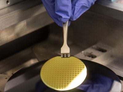
Double-gate qubit built on 300mm wafer 28nm FDSOI. Source: Leti.
“For the last 40 years or so the research into quantum computing focused on quantum wells in III-V compound semiconductors. But in the last 10 years or so the research has started working on silicon. Leti has reported a qubit built using 28nm FDSOI on a 300mm wafer; in fact a pair of quantum devices coupled by a tunnel junction.”
The use of silicon holds out the prospect of more affordable quantum computing and hybrid quantum/conventional computing because of potential compatibility with CMOS. “And silicon quantum computing can reuse a lot of the engineering from nano-electronics,” said Reita. However, quantum computing is unlikely to replace conventional computing or even achieve ubiquity in the near future, said Reita. This is mainly because for most materials it requires extreme low temperatures of less than 100mK to achieve sufficiently long electron-spin life times for quantum computing to take place.
Unfortunately, below about 4K CMOS tends to stop working with imbalances between the electron and crystal lattice temperatures, Reita said. “Dopants freeze and connections can become either superconducting or highly resistive.” So Leti is also working on cryogenic CMOS to ensure to interfaces between conventional computing and quantum computing are possible.
The challenges include moving from single and few qubits to multiple qubits and an understanding of how to limit the level of noise that requires quantum correction, Reita said. “In five years’ time we hope to have a quantum machine doing meaningful computing,” said Reita.
Next: Neuromorphics
Quantum computing is one of the novel computational architectures being pursued but another which has become red hot in industry and is already being deployed is neuromorphics. Leti is working hard to try and provide added value for research partners in this area.
The progress with Moores’ Law and parallelization in hardware architecture is now allowing a dramatic scaling up of neural networks to the point where the hardware can simulate networks with millions of neurons and billions of synapses. Up until now the selected architectures have been trained in the datacentre with huge datasets. Recurrent neural networks are effective for recognizing sequences such as speech while convolutions NNs use trainable convolution filters for image recognition, Reita explained.
Nonetheless the range of problems and architectural approaches is broad. In general, the more software-oriented the solution the less efficient it is but the more flexible and applicable. The more hardware-oriented the more efficient it is but the more case specific and the less flexible. “To recognize one person in a million you have to go to the cloud. But to tell the difference between a person and dog can be done small scale.”
One of the approaches Leti is looking at is how to address problems hierarchically. So that the same problem can be solved on the smartphone, on the television or in the cloud, Reita said.
Leti is part of a joint program spanning a number of research institutes within CEA Tech, including Leti and List. List is the Laboratory for Integration of Systems and Technology. The program is looking at the physical implementation of neural networks on dedicated circuits and memories made using advance silicon manufacturing. So this links back to novel devices and 3D integration including CoolCube, ReRAM as synaptic elements and FDSOI and nanowires.
And by way of design support Leti has developed a neural network design platform called N2D2 which can produce software and synthesizable hardware.

N2D2 internal tool for neural network design and optimization.
In terms of neural network design Leti has turned towards spiking architectures. That is one where neurons and synapses are modelled against time and communicate by emitting a series of signal spikes. The neurons do not all fire at each propagation cycle (as happens with multi-layer perceptron networks) but fire when the neuron reaches a specific value or state. The spike then pushes the state of connected neurons higher or lower and there may be an inherent decay function. Various schemes can be used to encode a real-value number, either relying on the frequency of spikes, or the timing between spikes.
“We can have a fully asynchronous system so when it is inactive no power consumption,” said Reita. “It’s easier to save power in analog and spiking systems.”
Next: Europe’s NeuRAM3
Leti is part of the NeuRAM 3 European collaborative research project that is developing the Dynamic Neuromorphic Asynchronous Processor Scalable-Learning (DynapSEL) for implementation in 28nm FDSOI. The design taped out in November 2016 and silicon is expected back this month of July.

Floor plan and specifications of DynapSEL chip. Source: Institute of Neuroinformatics of University of Zurich (Prof G.Indiveri) and NeuRAM3 project
For now DynapSEL has an SRAM on board. A lower-power version with non-volatile memory is due for delivery in the second phase of the program and by the end of 2018. As to what sort of non-volatile memory Reita said the decision is not yet final.
There are choices with different levels of maturity, ease of integration, and suitability to synapse behaviour. Filamentary OxRAM, such as hafnium oxide, is a favorite for reasons of ease of manufacturing integration, said Reita. Conductive bridging RAM (CBRAM) is a design favorite because voltage levels match CMOS and it is the lowest current. Finally there is chalcogenide-based phase-change memory (PCM), which appears to be an industry favorite with Intel now introducing its 3D Xpoint memory, said Reita.
To conclude Reita pointed out that challenges with Moore’s Law scaling over the past few years is increasing the opportunities for research but also prompting institutes to focus – and in part gamble – on where they can add the most value. Rieta is pleased that some of Leti’s choices made four years ago are now starting to pay off.
“The way we decided to go now seems to be more widely accepted. Shrinking is used up for the main part but there are a lot of possible alternatives. We are coming into an era of system optimization again. And that is why system companies are re-aggregating things.”
Related links and articles:
News articles:
CEA-Leti operates qubits in CMOS
Quantum computing startup has $69 million
Time is ripe for machine learning, says IMEC
Report: Apple working on neural processor
 If you enjoyed this article, you will like the following ones: don't miss them by subscribing to :