VTT develops printable e-nose sensor
Periodic optical nanostructures, known as photonic crystals when they affect the motion of impacting photons, can be implemented as nano-structured surfaces. Such nano-structured surfaces find use in so-called Surface Enhanced Raman Scattering (SERS) instrumentation, capable of characterising very accurately the chemical composition and structure of materials, in any state.
The surface-sensitive technique relies on precisely nano-engineered structures plated with gold, which have the effect to enhance transitional Raman photon scattering at a set of frequency bands unique to each material (like a signature of its chemical composition and state).
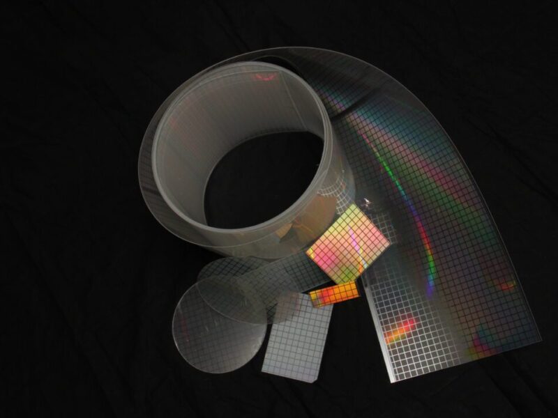
Until recently, such nanophotonic structures were difficult or expensive to manufacture in large volume. This challenge was addressed by the Photosens consortium using roll-to-roll (R2R) nanoimprinting methods. The photonic crystal sensor was demonstrated first at wafer level then at sheet-level using tailored polymer materials – see figure 1.

Fig. 1a: Roll-to-roll printed polymer SERS structures and gold coated SERS chips with two different form factors.

Fig. 1b: Photonic Crystal structures replicated into a polymer material.
Nanoimprinting, also known as nanoimprint lithography (NIL) consists in pressing a micro-structured mold against a substrate coated with a moldable material. After deformation of the material, the coating is UV-cured and the mold is separated to leave a perfect replica.
Of course the initial mold could be engineered through optical lithography, but in this case it was provided by commercial partner 3D AG in the form of a nickel shim recombined from various masters structured using electron-beam lithography.
Then the shim was attached onto a reel for the roll-to-roll UV imprinting machine to manufacture the nanophotonic sensor structures at high-throughput, in effect, nano-texturing large-area plastic films – see figure 2.

Fig. 2: UV R2R nanoimprinting process
Special polymer materials were also developed, including functionalized molecularly imprinted polymers (MIP) to optimize sensor sensitivity and selectivity.
Project Coordinator and Research Professor for Photonics Solutions at the VTT Technical Research Centre of Finland, Dr. Pentti Karioja explained eeNews Europe that even with a sensitivity of an order of magnitude lower than the commercial reference, the photonic crystal sensors obtained have the potential to meet the initial target of formaldehyde detection in air. Formaldehyde is a common indoor air pollutant found in virtually all homes and buildings.
Using a R2R process on roll batches 400m long by 0.3m wide, sensor chips could be mass produced in tens of thousands of units costing less than €1.5 each. For the SERS sensor, a gold metallization further enhances the Raman scattering effect. At the moment, this would drive the price up to around 3€ per individual sensor, but it could be driven lower using R2R metallization.

Further material and process optimization could still lower cost. Functionalized nano-structures could be tailored to detect specific chemical compounds, to build multiple gas sensing chips at much lower cost.
Disposable SERS sensor and photonic crystal sensor read-out concepts were elaborated by the consortium. The SERS sensor can be read out using a commercial Raman reader, which is still quite an expensive instrument, but for the photonic crystal sensor, a table-top readout unit was developed using a commercial CCD camera and a fiber pigtailed laser source.
This way, the disposable polymer chip is placed in a cartridge for easy and repeatable alignment of the sensor chip with the excitation laser and CCD readout. A waveguide sensor based on the Young interferometer principle was also manufactured using the R2R process, read out by a similar type of reader which would be about ten times cheaper than conventional Raman readers.
Other partners in this project included the University of Southampton (UK), Momentive (Germany), TNO (the Netherlands), University of Vienna (Austria), Nanocomp (Finland), 3D AG (Switzerland), Philips (the Netherlands) and Renishaw Diagnostics (UK).
Visit PHOTOSENS at www.photosens.eu
Related articles:
‘Nose in clothes’ sensor for wearable electronics detects illness and fatigue
Towards small autonomous electronic nose devices
 If you enjoyed this article, you will like the following ones: don't miss them by subscribing to :