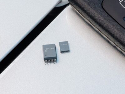

Wafer maker joins GaN-on-Si research
Such wafers are being hailed as useful for the production of power semiconductors and LEDs. In particular the research is looking to develop production on 200-mm diameter wafers with enhanced properties and reduced production costs.
Gallium nitride combines superior electron mobility, high breakdown voltage and good thermal conductivity. Structures with GaN/(Al)GaN layers evidence a very efficient switching behavior, according to IMEC.
To be commercially competitive with silicon alternatives it needs to become available on large diameter wafers and the IMEC program is looking to develop production methods for epitaxial deposition of GaN/(Al)GaN structures on larger-diameter silicon wafers.
In addition to Siltronic, other participants including integrated device manufacturers (IDMs) and foundries are also involved in the project, IMEC said.
"Siltronic has an enormous amount of experience in epitaxial deposition on silicon wafers that will increase the momentum of our GaN program to deliver a manufacturable GaN technology on 200-mm silicon wafers," said Rudi Cartuyvels, vice president of R&D Business Lines at IMEC, in a statement.
"Siltronic is already the world market leader for silicon wafers used to manufacture discrete and integrated power devices," said Ruediger Schmolke, senior vice president of technology at Siltronic, in the same statement. "This research project will help us to further consolidate our leadership position in this market."
 If you enjoyed this article, you will like the following ones: don't miss them by subscribing to :