First LPDDR6/5X 14.4-Gbps memory IP targets AI infrastructure
Cadence has taped out the industry’s first LPDDR6/5X memory IP system optimised to operate at 14.4Gbps, which is up to 50% faster than the previous generation of LPDDR DRAM.
The new Cadence LPDDR6/5X memory IP system is a key enabler for scaling up AI infrastructure to accommodate the memory bandwidth and capacity demands of next-generation AI LLMs, agentic AI, and other compute-intensive workloads across various verticals. Multiple engagements are currently underway with leading AI, high-performance computing (HPC) and data centre customers.
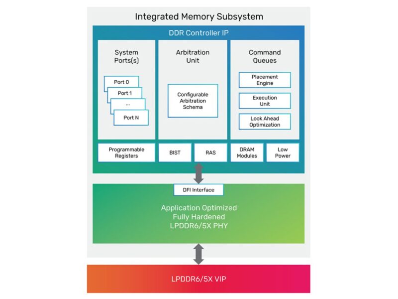
The Cadence IP for the JEDEC LPDDR6/5X standard consists of an advanced PHY architecture and a high-performance controller designed to maximise power, performance and area (PPA) while supporting both LPDDR6 and LPDDR5X DRAM protocols for optimal flexibility. The memory IP system supports native integration into traditional monolithic SoCs as well as multi-die system architectures by leveraging the Cadence chiplet framework, enabling heterogeneous chiplet integration. The chiplet framework, including the previous LPDDR generation, was successfully taped out in 2024.
“The evolution of data centres from HPC compute virtualisation to AI training and inference at scale has driven a massive buildout of AI infrastructure, and designing for efficient data movement via memory interfaces has never been more crucial. LPDDR6 has emerged as a key enabler of accelerated computing, providing the speed, bandwidth, power profile and capacity needed to perform AI inference efficiently,” said Boyd Phelps, senior vice president and general manager of the Silicon Solutions Group at Cadence. “With this tapeout, Cadence is continuing our track record of memory IP leadership by offering an industry-first LPDDR6 implementation delivered as an integrated subsystem optimised for customer applications.”
The complete PHY and controller memory system boasts a new high-performance, scalable and adaptable architecture based on Cadence’s proven and highly successful DDR5 12.8Gbps, LPDDR5X 10.7 Gbps and GDDR7-36G product lines. This first offering in Cadence’s new LPDDR6 IP product line supports the LPDDR6 and LPDDR5X standards, including LPDDR5X CAMM2.
The LPDDR6/5X memory IP system is suitable for the AI, mobile, consumer, enterprise HPC and cloud data centre markets. The IP provides maximum flexibility for end products, offering a range of performance, capacity, and cost targets to ensure long production runs. The LPDDR6/5X PHY is customisable for different package and system topologies and is available as a drop-in, hardened macro to provide fast and reliable integration, as well as rapid time to market.
The Cadence LPDDR6/5X controller provides a comprehensive set of industry-standard and advanced features for memory interfaces, including support for the Arm AMBA AXI bus. The memory controller is delivered as a soft RTL macro for maximum flexibility in terms of features, power, area, and performance.
The Cadence LPDDR6 memory IP system includes the LPDDR6 Memory Model, which enables engineers to perform comprehensive verification and ensure that system-on-chip (SoC) designs are compatible with the latest JEDEC interface standard, accelerating their adoption of this new technology with confidence. The LPDDR6 Memory Model includes a complete set of protocol checks, functional coverage and a verification plan.
When combined with Cadence’s UCIe™-based chiplet framework, the new LPDDR6/5X IP and Cadence’s other leading memory and interface IP deliver an optimised solution that enables rapid chiplet realisation.
 If you enjoyed this article, you will like the following ones: don't miss them by subscribing to :