IMEC adds 2D semiconductor channels to logic scaling roadmap
The IMEC, the world’s leading research institute focused on semiconductor manufacturing R&D, has added 2D materials to its logic scaling roadmap.
The possibilities and challenges of using single atomic layer materials, as the semiconductor channel within a gate-all-around (GAA) transistor are discussed in an article written by César Javier Lockhart de la Rosa, program manager for exploratory logic at IMEC. In particular he discusses the use of transition metal dichalcogenides (MX2).
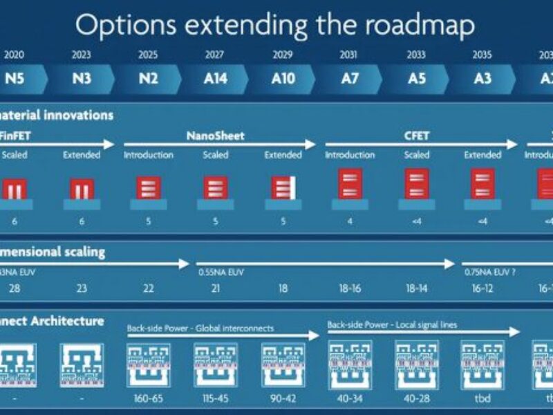
IMEC, work alongside industry partners, has already contributed much to the pre-competitive research on silicon transistor scaling.
It has proposed the extension of the industry-standard FinFET to GAA nanosheet transistors for high-performance computing applications. It has also recommended the use of backside power delivery in the process of being adopted.
Next on its roadmap is the complementary FET where further area efficiencies are created by stacking n- and p-type channels on top of each other. Imec foresees its introduction from the A7 node onwards, extending the IMEC technology roadmap to at least the A3 generation for introduction in about 2035.
IMEC is proposing that 2D-materials should then follow. But to prepare the way IMEC is proposing research into low-performance transistors used for simple peripheral switching in more immediate nodes.
But challenges abound with most of the conventional tasks in transistor manufacturing made more difficult or complex in relation to monolayer semiconductor materials.
These include:
- How to undertake 2D material deposition; high-temp deposition versus low-temp layer transfer
- Doping of 2D materials
- Finding a p-type material
- Dielectric layer and gate-stack integration
- Making low-resistance source/drain contacts
- Introduction into commercial fabs
Greater difficulty and complexity result in increased cost which scaling is seeking to reduce.
In the article IMEC’s Lockhart de la Rosa proposes the research institute will opt to phase 2D materials into less advanced nodes and in less performing devices. Starting at the A7 node and then moving to A3 to build up a body of knowledge prior to the full need for 2D materials. Part of this is driven by necessity as the A2 node will likely require the introduction of 0.75 numerial aperture extreme ultraviolet lithography – a technology that itself has not yet been developed.
IMEC has demonstrated a MX2 dry transfer process with excellent yield and reported it at the VLSI Symposium in 2024.
Related links and articles:
News articles:
BeDimensional gains €20 million to make 2D materials
Most energy-efficient transistor yet, made from two 2D materials
Paragraf gears up for next phase of graphene development
Black Semi raises €250 million for graphene pilot wafer fab
 If you enjoyed this article, you will like the following ones: don't miss them by subscribing to :