SK hynix unveils AI-NAND storage strategy at OCP Global Summit
 Cette publication existe aussi en Français
SK hynix has revealed its next-generation AI-NAND storage roadmap aimed squarely at the booming AI inference market. The company presented its new AI-optimized NAND storage lineup, the “AIN (AI-NAND) Family,” during the 2025 OCP Global Summit in San Jose, California, held from October 13 to 16.
This development highlights how NAND flash technology is evolving to meet the speed, efficiency, and density demands of AI workloads — critical factors shaping the future of data centers and edge computing infrastructure.
Optimizing NAND for the AI era
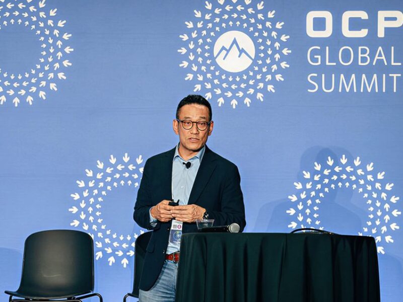
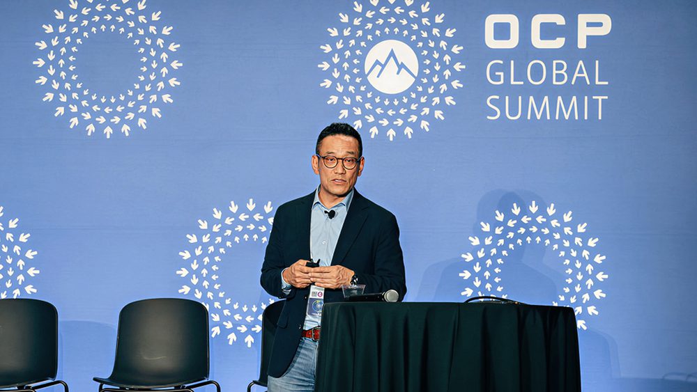
During the event’s Executive Session, Chun Sung Kim, head of eSSD product development at SK hynix, outlined the company’s AIN Family lineup — a trio of NAND-based solutions optimized for performance, bandwidth, and density.
AIN P (Performance) targets large-scale AI inference workloads by minimizing data bottlenecks between storage and AI processors. By redesigning both NAND and controllers, SK hynix aims to significantly improve processing speed and energy efficiency. Sample releases are planned by the end of 2026.
AIN D (Density) focuses on ultra-high-density, low-power storage for large datasets. The company plans to scale density from the current terabyte (TB) level to petabyte (PB) capacities, creating a mid-tier solution that blends SSD performance with HDD-like cost efficiency. This approach builds on advances in QLC (quad-level cell) NAND technology, which allows more data to be stored in the same physical space.
AIN B (Bandwidth) leverages SK hynix’s proprietary HBF (High Bandwidth Flash) technology to expand data throughput by vertically stacking multiple NAND layers. By integrating the stacking concept of HBM (High Bandwidth Memory) with cost-efficient NAND, SK hynix is aiming to close the performance gap driven by ever-larger AI models and growing inference workloads.
Building a NAND ecosystem for AI
To strengthen collaboration in the emerging HBF ecosystem, SK hynix co-hosted “HBF Night” with SanDisk during the summit. The event followed the companies’ memorandum of understanding (MOU) signed in August to promote standardization of HBF technology. The networking event at The Tech Interactive in San Jose drew industry architects, engineers, and researchers, who discussed joint strategies to accelerate NAND innovation for AI systems.
Ahn Hyun, president and chief development officer at SK hynix, emphasized the company’s long-term vision, stating:
“Through OCP Global Summit and HBF Night, we were able to showcase SK hynix’s present and future as a global AI memory solution provider, thriving in a rapidly evolving AI market. In the next generation NAND storage market, SK hynix will collaborate closely with customers and partners to become a key player.”
Accelerating AI storage innovation
SK hynix’s AI-NAND strategy reinforces its ambition to lead in the next wave of AI-driven memory and storage innovation. As data center operators and AI developers seek faster, denser, and more power-efficient storage, the company’s AIN lineup could help bridge the gap between traditional NAND flash and high-performance AI memory technologies.
With its strong track record in HBM and NAND development, SK hynix appears well-positioned to shape the architecture of AI storage systems for the coming decade.
 If you enjoyed this article, you will like the following ones: don't miss them by subscribing to :