Applied gets copper wiring to work on 2nm node
Applied Materials Inc. (Santa Clara, Calif.) has shown the use of ruthenium lining in high volume production enables copper interconnect to be scaled to the 2nm node and beyond.
The company has also introduced an enhanced low-k dielectric material to reduce chip wiring capacitance and strengthen logic and DRAM chips for 3D stacking.
Low-k dielectrics and copper have been used in ICs for many years. However, as monolithic integration goes to smaller dimensions the thinner dielectric material renders chips mechanically weaker, and narrowing the copper wires creates steep increases in electrical resistance, which increases power consumption.
At previous nodes Applied’s Black Diamond material has been used to surround copper wires with a low-dielectric-constant film. The latest enhancement to that material is Black Diamond PECVD [Plasma-Enhanced Chemical Vapor Deposition]. It reduced the minimum k value while offering increased mechanical strength to allow logic and memory die stacking.
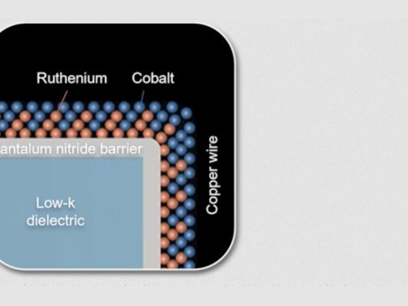
Applied has also formally announced its latest liner-barrier materials system although it is already in use at the 3nm node. It is a binary metal combination of ruthenium and cobalt (RuCo), which simultaneously reduces the thickness of the wiring liner by 33 percent to 2nm, produces better surface properties for void-free copper reflow, and reduces electrical line resistance by up to 25 percent to improve chip performance and power consumption.
“The AI era needs more energy-efficient computing, and chip wiring and stacking are critical to performance and power consumption,” said Prabu Raja, president of the Semiconductor Products Group at Applied Materials, in a statement. “Applied’s newest integrated materials solution enables the industry to scale low-resistance copper wiring to the emerging angstrom nodes, while our latest low-k dielectric material simultaneously reduces capacitance and strengthens chips to take 3D stacking to new heights.”
Related links and articles:
News articles:
Tall metal can almost halve IC’s line resistance, says IMEC
Researchers advance porous dielectric for better chips
Ruthenium shows the way to 2nm
 If you enjoyed this article, you will like the following ones: don't miss them by subscribing to :