CEO interview: AI creates step change for lithography. Aki Fujimura, D2S
AI and GPUs are fundamentally changing the way leading edge chips will be built in future fabs, says Aki Fujimura CEO of D2S (formerly Design2Silicon). The Silicon Valley firm was founded in 2007 to develop technology using GPUs for making and checking the photomasks used in semiconductor lithography.
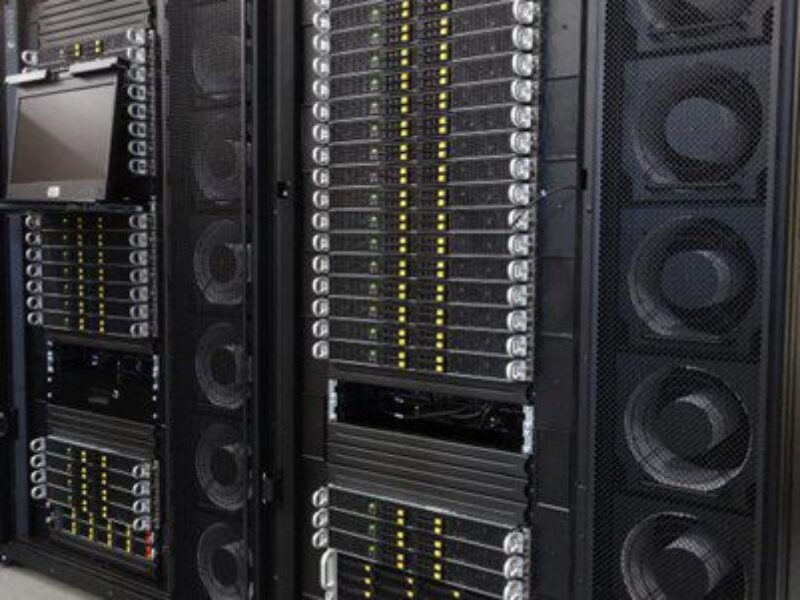
Making the masks uses electron beam systems and the checking has to deal with increasingly complex geometries. The company has just shipped its 50th system, with over 3,000 GPUs shipped in its Computational Design (CDP) systems. This represents a combined total of more than 50 PetaFLOPS of single precision (SP) processing speed says the company.
- Petaflop era for semiconductor manufacturing
- Nvidia boss pitches generative AI for chip manufacturing
- eBeam Initiatitive expands membership
GPUs optimised for single instruction, multiple data (SIMD) operation have been a key technology for graphics and AI, and D2S has also taken advantage of this, Fujimura tells eeNews Europe. The increased performance of GPUs is enabling new curvilinear techniques for masks, and this will change the way chips are designed, he says.
“SIMD is different from a CPU as you have many processors that are executing the same instruction. That’s good for a number of things, such as any simulation of nature, e-beam simulation or lithography simulation,” said Fujimura. “It is also the case that GPUs are great for image processing and for AI. When AI came along it specifically took advantage of SIMD computing and the fact that it continues to scale by bit width rather than the clock speed. Because the bit width continues to scale, that’s the thing that’s driving the AI innovation. So all of these are good for us.”
“One side of what we do is creating the mask shapes. The designers use the EDA tools to target what should be on the wafer and at 3nm and 2nm these are difficult to achieve reliably,” he said. “Reducing the statistical variation is incredibly important for manufacturing and there are many techniques for creating the shapes on the masks and these make the masks much more complicated.”
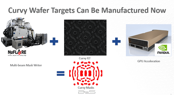
“If the target shape is curvilinear the SIMD approach is perfect as the same GPU can process any shape with the same accuracy and speed whereas CPU-only computing will be a function of how complex the shape is.”
“What’s happening in the mask making world at advanced nodes, because multibeam mask makers became available a few years ago and the leading edge fabs have many machines, they are able to produce curvilinear shapes and the way that you can best compute those shapes is with GPU acceleration.”
“Curvilinear mask making is now a practical reality thanks in part to GPU acceleration. Now that the mask manufacturing chain is ready for curvy, it’s time for the EDA infrastructure to rethink the Manhattan assumption of chip designs. With the power of GPU computing and the ability to manufacture curvy design features, the door is finally open for curvy design tools to enable even better manufacturing-aware designs.”
The ‘curvy design’ is Inverse Lithography Technology (ILT) which manipulates the shapes to produce the target mask shapes for the target wafer design.
“The second things is to take that mask shape and produce what is good for the wafer. This gives rise to MPC, or mask process correction, taking the mask production and making sure the mask is producing the design you want. Particularly for multibeam machines GPU is very appropriate.”
D2S also develops tools that provide in line MPC correction inside a machine, the NuFlare MBM-2000.
“We also do simulation of the wafer and of the mask, as well as verification for mask rule checking MRC which is similar to DRC for geometry checking,” he said.
Deep learning applications
D2S has been working with Mycronic in Sweden and NuFlare Technology in Japan on a range of 30 deep learning (DL) applications for semiconductor manufacturing. “We are in the process of putting DL into products,” said Fujimura.
“There are many places where deep learning can help,” he says. “One place is anything that is iteratively optimised and ILT is a space that is iteratively optimised. Anything where there is evaluation the accuracy of that evaluation given a specific time constraint can be enhanced using deep learning.”
“Completely separately, anything analysing pictures such as recognising anomalies can be a very useful applications and this happens when you inspect a mask. That’s massive amounts of data and you are looking for anomalies and that is the kind of thing that machines are good at. Deciding what kind of error it can be is something deep learning can help with.”
“Another interesting area is machine prediction for maintenance needs. The machines need to be maintained over time and being able to automatically diagnose issues from the images to identify components that are causing the problem, so the speed of service is accelerated.
Security
Security is key for mask makers so access to cloud-based GPUs is not an option.
“In our case we provide a platform so its not on the cloud. Mask shops have a lot of concerns over data security. They are dealing with customer designs and want to make sure that is secure so they have their own on premises cloud,” he said. “The trend is for EDA to move to the cloud and that’s true in semiconductor manufacturing, but there is a lag compared to the rest of the computing world because of the data security.”
2nm masks
The company currently uses Nvidia’s A40 family of GPUs in its 7th generation of CDP machine. “We haven’t announced the 8th generation but the next set of GPUs are already available and we will be using those in the future,” he said.
“The next generation of mask writers need to be even more precise and that requires more computing but as the task gets more difficult the computing gets faster. The L40 compared to the A40 has 2.4x the throughput,” he said.
Aki Fujimura is moderating the panel, “Why is Curvy Design an Opportunity Now?,” at the 60th Design Automation Conference (DAC) in San Francisco on Tuesday, July 11, 2023 from 1:30-3:00pm PDT at Moscone West, Room 3014.
 If you enjoyed this article, you will like the following ones: don't miss them by subscribing to :